20
\$\begingroup\$

I've designed several PCBs where I needed to keep the ground returns of different parts of the circuit separated, i.e. analog, digital and high power. I use Cadsoft Eagle for schematic capture and layout. It is easy enough to define different ground symbols in the schematic editor. They each have their own net name. However, the grounds must all eventual be connected at one point on the PCB to define the overall ground reference. When connecting one ground (or supply) to another, Eagle generally overrides one of the net-names with the other, i.e. removing their distinctiveness. This is sensible from a idealistic electrical viewpoint that assumes that the wires have no impedance. However, in the real world there is no such as zero impedance, or ground for that matter! This net-name overriding behaviour is getting in the way of PCB design. How do I work around this behaviour? This isn't a big problem in the schematic drawing because the supply symbols are retained and the net names are hidden. However, in the layout editor, after connecting grounds, only one unique ground net-name remains.

It is possible in the layout to manually keep the distinct grounds separate even though they have the same net name, and to connect them at one point. Thus it is still possible to achieve the design goal with only one uniquely deified ground. However, it is a logistical nightmare keeping the distinct ground traces separated when they have the same net-names.

Is there a better way to do this?

I have tried making my own Eagle part where the multiple and distinct grounds connect electrically, but, do not have the same net-names. The part was just a series of physically overlapping SMD pads. Each pad could be connected to a unique net-name thereby preserving the distinct grounds, but, it provided an electrical connection between the grounds. This seemed to work well with the drawback that the Design Rules Check (DRC) thought that the overlapping pads were a problem. In fact, Sparkfun has an eagle part that does this, however, they opted to keep the pads separated, i.e. not overlapping. This solves the DRC problem, but, then the board is then not connected properly electrically. This caused bugs in one of my boards before.

Is there a good solution to this problem? Is Eagle weird in its handling of this? Do other EDA tools do better than Eagle in handling this? I am doing something wrong? This has been a source of irritation for me for some time now.

\$\endgroup\$
6
  • 4
    \$\begingroup\$ I don't know Eagle, but when you define a footprint, is it possible to draw copper that isn't a pad? Then you could tie your pads together without triggering the DRC rule for overlapping pads. Altium has a special category of part that does this. \$\endgroup\$
    – The Photon
    Commented Dec 11, 2011 at 1:09
  • \$\begingroup\$ @ThePhoton: Good suggestion. I tried this just now. It didn't work. I can't overlap the copper polygon with the pad or I get overlap DRC errors. I tried making it so only the edges of the pad and the polygon overlapped, but, then I get clearance DRC errors. It is still not a clean solution. Maybe the solution is to get Altium! lol.. \$\endgroup\$ Commented Dec 11, 2011 at 2:22
  • 1
    \$\begingroup\$ What I'm actually used to doing is just use one name for the ground net, and just know which parts need to be in semi-isolated areas. You may be able to define placement "rooms" for your components to help keep track. \$\endgroup\$
    – The Photon
    Commented Dec 11, 2011 at 2:55
  • 1
    \$\begingroup\$ I have seen layouts with separate digital and analog grounds where they were connected in one spot via a 0-ohm resistor. This added less than a cent to the BOM and kept the nets separate. \$\endgroup\$
    – tcrosley
    Commented Dec 11, 2011 at 4:37
  • \$\begingroup\$ @ThePhoton: I like the idea of just separating components into different "rooms" to keep everything straight. This is a good idea and is consistent with the article on signal integrity "Use one solid unsplit ground plane, by Henry W. Ott". However, there are some components that will have both a digital and analog ground. But, I think overall this method is good practice anyway. \$\endgroup\$ Commented Dec 11, 2011 at 17:00

6 Answers 6

10
\$\begingroup\$

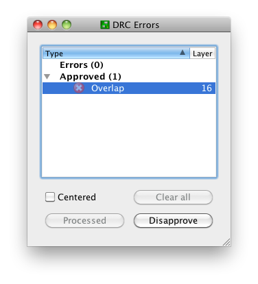
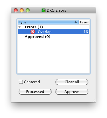
Create a footprint with GND and AGND pads. Draw copper between these pads. Yes, this will produce a DRC "Overlap" error as shown below:

DRC "Overlap" error in errors dialog

This is OK. There three buttons at the bottom:

  • Clear all
  • Processed
  • Approve

"Clear all" will temporarily clear the list for this run of the DRC. I'm not sure why that's useful; just close the window if you want it shortened.

"Processed" will fade out the color of the red X. This is potentially useful if you're iterating through a long list of DRC errors and fixing them as you go; you can keep track of the ones you think you've corrected.

"Approve" is the only one I use on a regular basis. This moves the error from the errors list to the approved list:

Error moved to approved list in errors dialog

and keeps it there on subsequent runs of the DRC. Note that this only moves this specific error with this specific pair of nets at this specific location. Closing this window and running the DRC again produces the notification "DRC: 1 approved errors"

DRC: 1 approved errors

and no "DRC Errors" dialog. You can get this dialog back by creating an error, or (preferably) the errors command, the yellow exclamation point in the above screenshot, or the menu Tools -> Errors.

The "Approve" functionality exists for a reason, the same reason that we have tools like

#pragma GCC diagnostic ignored "-Warning"

Sometimes, it's OK to ignore a DRC error. This is one of those times.

\$\endgroup\$
1
  • \$\begingroup\$ Thanks. I felt like I was sweeping the problem under a rug by approving an error. It seems stronger that dismissing a warning! But, I see that they are equivalent. This may be the best solution. I think Eagle should include such a part as Altium does without the DRC errors. But, if that is the cleanest solution then we don't have much choice given that we are using lower end software. \$\endgroup\$ Commented Dec 11, 2011 at 17:04
6
\$\begingroup\$

I do this with special devices I have created for this purpose I call "shorts". These are abutting pads and don't require any components to actually be installed. In the schematic they show up as a slightly thickened line. The point is they look like a connection in the schematic with just enough distinctiveness to see but hopefully not get in the way. Since they are separate devices from Eagle's point of view, you can place them where you want like any other device. You can see such a short at the bottom of page 1 of the USBProg schematic. That particular one has the component designator SH2, and is the single connection point between the power ground and the main board ground.

My shorts are freely available in the Eagle Tools release at www.embedinc.com/pic/dload.htm. There are various shorts depending on which layer you want them on or whether they cross layers.

The one drawback in Eage is that you will get a lot of nuisance DRC errors for every short. I hear that in version 6 it will be possible to tell it in the package that certain things are allowed to overlap, but as of now there is no way around this.

\$\endgroup\$
4
\$\begingroup\$

Multiple ground planes are absolutely necessary. With full respect to Mr. Ott since everything he says is not wrong per se, he just reaches an incomplete conclusion because of omission of consideration of the analog side. The point that Mr. Ott is missing is that within the analog section itself, multiple ground planes - one for each functional block of analog circuitry - arranged in a star-ground pattern, is a requirement for low noise (Douglas Self "Small Signal Audio Design" Focal Press 2010, NwNavGuy http://nwavguy.blogspot.jp/2011/05/virtual-grounds-3-channel-amps.html). While these two references specifically consider audio designs, the principles are even more important in high precision analog circuitry in data acquisition and/or control applications.

The issue then becomes: how do we implement digital ground within a design possessing multiple analog grounds? A mistake is to "blap" the PCB with a single ground plane and use only the layout techniques described by Mr. Ott to avoid interference between analog and digital sections. If you do this, analog performance may suffer because of analog-to-analog interference.

In a typical design, each ADC or DAC will likely be related to different functional sections of the analog circuitry. Provide an analog ground "island" for each of these sections with an independent ground return path, arranged in a star-ground pattern, back to the "reference ground." This reference ground is not necessarily the power supply (or battery) ground. If there is a regulator supplying the analog power then the reference ground is the ground pin of the regulator IC. As to the digital side, the ground pin of the regulator powering the digital side (if different from that supplying the analog side) should also be tied back to the reference ground with traces as short as possible. Digital ground should also be implemented as an isolated island with an independent ground return back to the reference ground.

Now we have to deal with the interface between analog and digital sections. This includes

  1. separate analog and digital grounds on ADC and DAC devices,
  2. separate supplies for analog and digital power on the same device and
  3. control lines such as I2C or PCI buses.

(1) Separate analog and digital grounds.
Designers of mixed signal IC's know that analog and digital ground should be connected together but they cannot provide that connectivity inside the IC due to restrictions of the geometry of the die and pad connections. Thus the recommendation is always to connect these two points externally as close to the IC as possible. Note that this is not always the case - many DAC and digital potentiometers (a form of DAC) do not have separate analog and digital ground pins. For these devices, the connection has already been made inside the IC. When connecting analog and digital ground together, the combined pair should be connected to the analog ground plane for that section of the circuit.

(2) Separate analog and digital supplies on the same device
These power planes will be separate even if they happen to be the same voltage. The digital power plane should be isolated from its source regulator (and analog power if driven by the same regulator) by way of a ferrite bead. Connect digital power of mixed signal IC's to the digital power island; at a minimum, bypass both analog and digital supply to the ground pin of the IC with ceramic capacitors (100nF X7R/X5R are recommended, some IC manufacturers recommend additional capacitors - follow any guidelines stated in the data sheet). Follow best practice layout guidelines by locating the bypass capacitors as close to the device pins as possible. Ensure that the digital bypass capacitor is connected to the combined analog and digital ground on the digital ground pin side; it should not connect somewhere "in between" the analog and digital pins. Recall that the digital supply bypass capacitor is in fact there to source the current pulses that occur when the digital devices switch state. Thus there is an AC current loop from digital supply pin, through the capacitor, into the ground pin (digital side) and back through the device to the digital power pins - a current loop that can and will emit radiation. This is why it is important to place the bypass capacitor as close to the device as possible thereby minimising the size of this current loop.

(3) Control lines such as I2C and/or PCI busses
So far, given the above, we have a problem connecting control lines from, say, the micro-controller to the mixed signal devices since these lines must, by definition, cross from the digital side to the analog side. For this, follow Mr. Ott's recommendation of providing a bridge between analog and digital ground. For each analog island that has control lines connecting it to the digital side, provide a bridge from each analog ground to digital ground and route the signal lines directly over that bridge. Depending on the actual layout and circuit complexity, you may have a single bridge connecting to more than one analog ground. That is acceptable - the key issue is to route all the noisy control lines over a bridge. The reasons for this are fully explained in Mr. Ott's article.

Summarising, the above techniques are more work than a single ground plane but are necessary. None of the above discussion negates or removes Mr. Ott's directions on careful layout and always knowing where the DC and AC current paths are flowing (both paths - send and return). Most auto-routers will have trouble providing a quality outcome with the above in mind. You will always have to perform some routing by hand - a possible time-saving technique is to auto-route the circuit islands and hand-route the interconnections, ground returns, power distribution, control lines. Some PCB layout applications have weak support for creating the analog-to-digital ground bridges since it is effectively connecting different signal nets. If your software has explicit support for this, great, if not you might be forced into a situation where you override an error detected by the DRC process.

\$\endgroup\$
0
2
\$\begingroup\$

"Is there a better way to do this?"

Yes, there are two ways to handle this:

I'm not sure how you do it in Eagle, but in Altium people make the "virtual short" component very similar to what you already described. You mention the dilemma: Making the pads overlap on the "virtual short" component, alas, gives a DRC error. Making the pads separated on the "virtual short" component, alas, makes the sections not properly electrically connected. There is a third choice, a solution to the dilemma:

Make the pads of the "virtual short" component extremely close to each other, but not overlapping -- 0.002 mil (2 microinches) short of contact. Then fix the DRC rules so that, for this one special component, they don't give a clearance error. Such a microscopically small gap can't actually be fabbed on a PCB -- in production it will end up shorted, as you desired.

Is there any way to see if perhaps Henry Ott is right, and one single uninterrupted ground plane for everything -- analog, digital, and power -- might work best?

\$\endgroup\$
3
  • 1
    \$\begingroup\$ No, one single ground plane for everything is not a good idea in a lot of cases. Ott seems to be saying not to split the ground, which I agree with, but that is different from having localized grounds that are utlimately directly connected to the main ground. There are lots of good reasons for doing this. Your answer seems to have misinterpreted something and then turned it into a bad recommendation. If not misinterpreted, then Ott is just plain wrong, and thereby you are too. \$\endgroup\$ Commented Dec 11, 2011 at 14:53
  • 1
    \$\begingroup\$ The original poster seemed to be talking about connecting AGND and DGND together at one and only one point, a practice that Burr Brown, "Analog-to-Digital Converter Grounding Practices Affect System Performance", specifically points out as inferior to a single solid ground plane. I realize I have a lot to learn. I'm curious -- what are these "lots of good reasons" for something other than a solid ground? Would you mind giving me a reference to a book or web page that lists those "good reasons"? \$\endgroup\$
    – davidcary
    Commented Dec 12, 2011 at 14:07
  • \$\begingroup\$ It's mostly about isolating the nasty loop currents you don't want running accross the main groundplane where they can cause offset voltages and radiate. I discuss some of these issues at electronics.stackexchange.com/questions/15135/… \$\endgroup\$ Commented Dec 12, 2011 at 15:20
0
\$\begingroup\$

A bit late but still, here is how to do it:

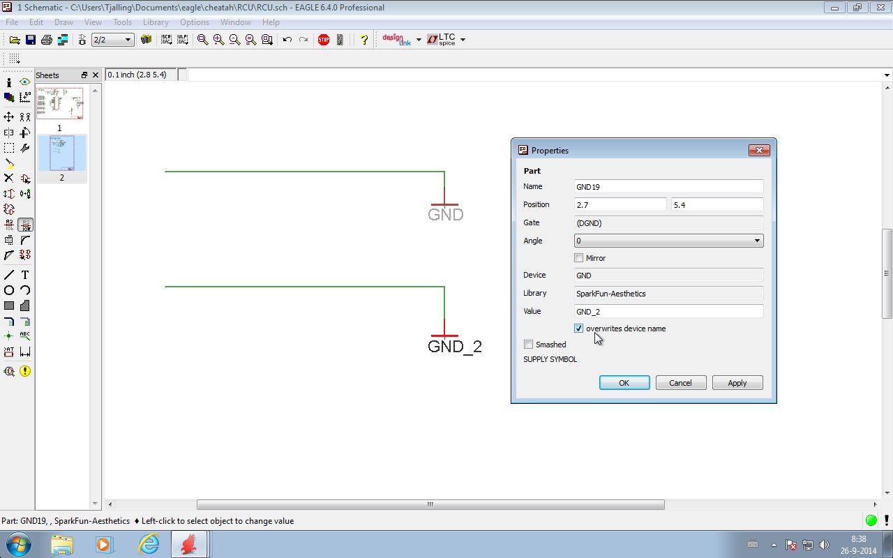
To get 2 different grounds is simple. Add a ground symbol in your schematic, then give it a new value. Now go to the properties of that ground symbol and an extra option will be available which says 'overwrite device name'. Uncheck that option.

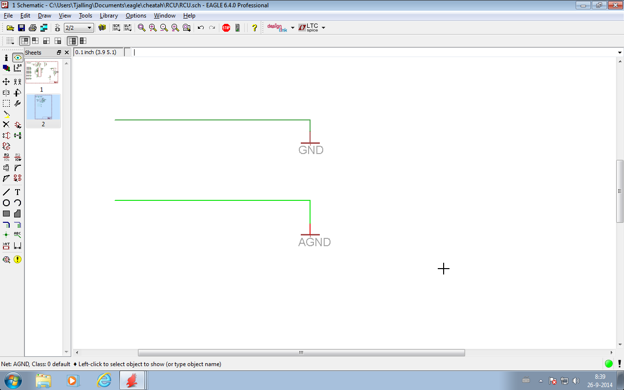
Now draw a net wire to the ground symbol and name that wire AGND for example. Now your ground symbol will have the same net name. Now give your ground symbol a value again that says AGND to make it a bit more clear that that ground is AGND and not the other ground for example.

Below are some images to make it bit more clear. Look at the bottom left of the screen for signal names so you can see that it works.

enter image description here

look at the signal name at the bottom left of the screen

again look at the signal name at the botton left of the screen

\$\endgroup\$
1
  • 1
    \$\begingroup\$ that helps in the schematic, but does absolutely zero things in the layout editor, the layout editor will merge them as it was one ground, which for all intent and purposes you will never want, those grounds are kept separate for a reason \$\endgroup\$ Commented Nov 25, 2015 at 2:54
0
\$\begingroup\$

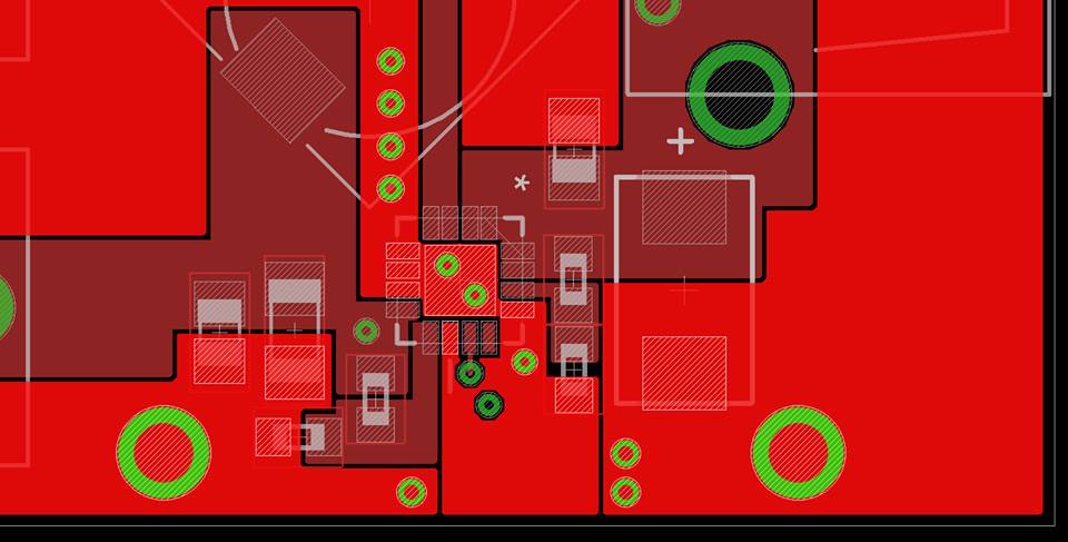
something that worked for me, was to shape the ground plane polygon geometry so that it's around the other plane

enter image description here

The ground planes are still connected thru one via one thru one the ICs pins, but since the nets have the same name, and since the geometry doesn't allow the fill, Eagle does not connect the two directly

\$\endgroup\$
1
  • \$\begingroup\$ that works, but is extremely labor intensive! \$\endgroup\$
    – user371366
    Commented May 23, 2017 at 7:50

Your Answer

By clicking “Post Your Answer”, you agree to our terms of service and acknowledge you have read our privacy policy.

Not the answer you're looking for? Browse other questions tagged or ask your own question.