0
\$\begingroup\$

I'm really new to digital systems. I'm trying to understand the difference between control path and data path. As far as I understood data path is where all the operations regarding ALU and registers happen. In control path we basically controls the above mathematical operations and etc.

Imagine I have to make a simple block diagram of a system which does parallel to serial conversion. The operation is as follows

  • The conversion shall be started when a signal ENABLE is asserted for one clock cycle.
  • an output signal READY is asserted when the module is ready to accept new values.
  • an output signal DONE is briefly asserted when the conversion has been completed. Now I tried to add the above signals as input and output signals to the below block diagram which specifies it's control path or data path. Did I understand it correct? If it's wrong please explain it to me.

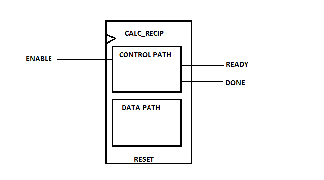
enter image description here

\$\endgroup\$
2
  • 1
    \$\begingroup\$ For parallel to serial conversion: the data path would be the actual part where the parallel goes in and serial comes out, the control path would mostly be the parts that control timing and synchronization. There isn't always a clear distinction between control and data, but I think there is in this case. \$\endgroup\$ Commented Jun 19, 2016 at 10:27
  • \$\begingroup\$ This concept extends to whole systems, incidentally: learningnetwork.cisco.com/thread/33735 \$\endgroup\$ Commented Jun 19, 2016 at 15:03

1 Answer 1

2
\$\begingroup\$

The simple answer is, yes, you've done it correctly. But it can get more complicated than that.

In a "normal" computer, control and data information are both sent along a common path between a storage and an execution unit. In a PC, storage is ROM and/or RAM, and execution is the CPU. (And yes, within the CPU data and control paths become separate - don't worry about it.)

This architecture is called a Von Neumann architecture, and is dominant in computers. However, it's perfectly possible to separate data and control from start to finish. This is called a Harvard architecture, and is sometimes seen, particularly in DSP systems. Probably the best-known current example is the Analog Devices SHARC line.

\$\endgroup\$
3
  • 1
    \$\begingroup\$ I have no quibble with the first paragraph. However control and data are not sent along a common path. Address, control and data are separate. I double checked the JEDEC DDR3 spec, and Micro Design guide, and all three are seperate at the package and DIMM level. Further a common or separate data and control isn't sufficient to charaterise Von Neuman vs Harvard Architecture. So I think the last paragraph is very misleading. IMHO it could be deleted without detracting from the answer. \$\endgroup\$
    – gbulmer
    Commented Jun 19, 2016 at 16:19
  • \$\begingroup\$ @gbulmer - Hmm. I'm trying to fit the answer to the OPs experience level. Although there are data, address and control lines involved in retrieving data from RAM and ROM, all of the CPU internal states (including implied address and control) in a program are specified in the retrieved data. It is in this sense that I was speaking. \$\endgroup\$ Commented Jun 19, 2016 at 17:45
  • \$\begingroup\$ Your answer introduced the computer, ROM and RAM as part of the explanation. I have no issue with removing all of that to simplify the level of the answer. However, IMHO if it is included, then it should be accurate, because other people may read it in the future. \$\endgroup\$
    – gbulmer
    Commented Jun 19, 2016 at 18:08

Your Answer

By clicking “Post Your Answer”, you agree to our terms of service and acknowledge you have read our privacy policy.

Not the answer you're looking for? Browse other questions tagged or ask your own question.