Could you provide an example about reading or writing data?
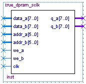
I'm not going to provide an example of code, this is clearly an academic exercise so I'll summarize it. First off, if your implementing this on real hardware, this is the wrong way to go about this. If using memory in real hardware, you need to find out what the fundamental memory blocks are for that device, which generally have a read, write, data lines and address lines and a clock. The one shown below is two port, which allows you to read\write to two different points in the memory in one clock cycle.

Source: https://www.intel.com/content/www/us/en/programmable/support/support-resources/design-examples/design-software/verilog/ver-true-dual-port-ram-sclk.html
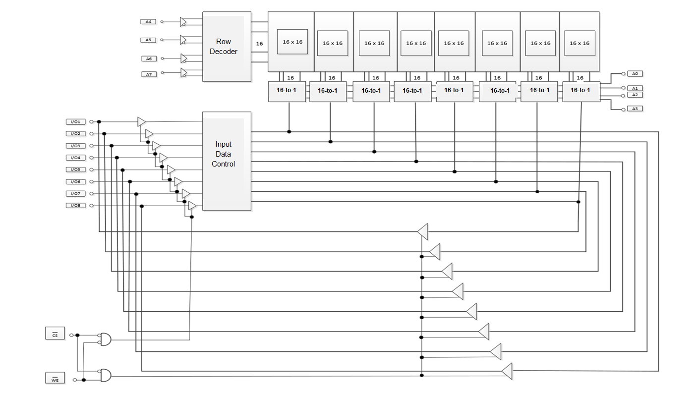
When writing, the first thing that needs to happen is the \CS line needs to go low and the \WE line needs to be low. This is to enable the buffers before the input data control block and disable the write buffers. Data then needs to be presented on the the I/O lines and the address changed.
It appears that the memory blocks are a 16x16x1 bit. Which means that all the lines to the memory block are address lines. This also means that the memory could be bidirectional and the 16 to 1 muxes also could be bi directional.
They wouldn't have to be bi directional however. If there is flexibility in the implementation of the design, the 16 to 1 muxes could be duplicated to have 1 read and one write mux then you could use memory that is not bidirectional.
When reading, the \WE line must be high and the \CS line low, this enables the read buffers.
The confusing thing is why they have buffers at all, as the data lines are bi-directional. This leads me to believe that they are actually using data two lines that are one way. This block diagram is poorly drawn.
In addition to this, what does determine the number of bits I use for the input of the Row Decoder?
Assuming that the memory blocks are 16x16x1 the row decoder will take 4 bits and select only one row from 16. I think it would be better to use a mux, for some reason there are not gates placed before the row decoder.
I know that for n bits in the input we get 2^n bits in the output of
the decoder. So here I get 16 bits. But why do I have 4 bits in the
input (A4,A5,A6,A7).
If it's a 16x16x1 ram (which is my assumption) then if there are 16 address lines that can only be turned one at a time, you need 4 bits to do the selection.


