1
\$\begingroup\$

Problem:

my photo diode recieves pulses of width 10ns-150ns and repeating at rate of 1Hz-50KHz

the current from photo diode depending on incident light can go from 10nA-100mA, so i have two photo diodes to cover the dynamic range, what i want to do is limit the current from a photo diode to 5mA lets say in one channel

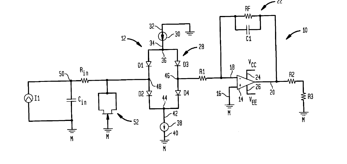
My application needs me to do current limiting, so for this i found a hope with this patent

which has the basic circuit as below

enter image description here

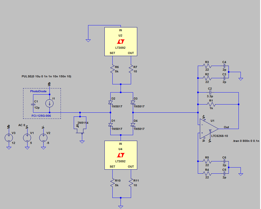
typically i want to replace the I1 with my photo diode and in the question here even i tried to realize the circuit with suggestions in answers and even got few decent results

but the problem is i am not able to make out this circuit in my mind in terms of current, when i observed in simulation the diode connected FET 52 does the job of discharging the excess current and current sources 30 and 40 are the saturation currents

fully realized circuit:

enter image description here

\$\endgroup\$
9
  • \$\begingroup\$ That patent is still active. Do not use that circuit unless you are able to pay any licensing fees. \$\endgroup\$ Commented Jul 1, 2016 at 4:50
  • \$\begingroup\$ @IgnacioVazquez-Abrams understand its a active patent, i want to understand this more than misusing it, if active patents are not to be discussed i would delete the question, please inform, i am less aware extent of discussing active patents \$\endgroup\$
    – kakeh
    Commented Jul 1, 2016 at 4:53
  • \$\begingroup\$ I'm sure that it's fine to discuss it, I am simply warning against putting it into production. \$\endgroup\$ Commented Jul 1, 2016 at 4:56
  • \$\begingroup\$ Are you saying you don't see the circuit working in LTSpice, or that the circuit works in LTSpice but you want an intuitive understanding of why? \$\endgroup\$
    – The Photon
    Commented Jul 1, 2016 at 5:25
  • \$\begingroup\$ I'm guessing it's the first, because you have not provided a positive supply voltage to the LT3092 chips to allow them to work as designed. Notice on the first page of the '3092 datasheet the requirement "Vin - Vout = 1.2 to 40 V". \$\endgroup\$
    – The Photon
    Commented Jul 1, 2016 at 5:26

1 Answer 1

1
\$\begingroup\$

How is the circuit supposed to work?

I'll refer to the designators in the patent drawing.

First, normal operation:

By KCL at node (36), the sum of the currents through D1 and D3 must be equal to the current provided by the current source (30). Similarly, the sum of the currents through D2 and D4 must be equal to the current sunk by current source (38).

Now when I1 produces a current, it will increase the current through D2 and decrease the current through D1. So that means the the current through D4 must decrease and the current through D3 must increase.

Now the current through D4 and D3 are not equal, so by KCL at node (46), some current must flow into the op-amp circuit through R1. This current will be equal to the current originally produced by I1.

Now, overload operation:

Because of current source (38) (let's call that "I38") the maximum current through D2 is limited. If the current from I1 is greater than I38, it can't flow through D2, and it can't flow through D1 because it would be reverse from the diode's direction. So the voltage at node (48) must rise until the JFET (52) is activated to pass current in diode operation, and the excess current flows through the JFET. Meanwhile, the current imbalance between D1 and D2 is limited to I38, so that is the current that gets delivered to the op-amp circuit.

Why is your simulated circuit probably not working?

According to the datasheet, LT3092 works when there is a positive bias of between 1.2 and 40 V between the input pin and output pin.

Your circuit provides no such bias. If the input node voltage (node (48) in the patent drawing) is positive, then your U4 might operate correctly, but U2 will not. If the input node is negative, then U2 might operate correctly, but U4 wil not.

A likely solution is to provide either a positive bias at the IN pin of U2, or a negative bias at the output of U4 (where R10 and R11 are joined).

\$\endgroup\$
10
  • \$\begingroup\$ very thanks for your explanation it solved my doubts and , but now i have a doubt, i just eliminated the current sources and the schottky bridge just left the diode connected JFET which gets in to play as soon as the voltage builds up at the inverting terminal of opamp, because when opamp saturates due to excess current, there will be an voltage built up at opamp inverting input , acc to my datasheet it should not exceed 2V, so this change has worked much better than this complete complex circuit, please let me know disadvantage with only FET approach, or may i put it as a new question? \$\endgroup\$
    – kakeh
    Commented Jul 2, 2016 at 4:11
  • \$\begingroup\$ it may be a simulation problem ? the above circuit still works as desired, but when i tried to put a +2.5 at IN of U2 or -2.5 at R10 and R11 joint, it resulted in a weird behavior of circuit and the results were in appropriate,i can post results in a new answer if you want \$\endgroup\$
    – kakeh
    Commented Jul 2, 2016 at 4:18
  • \$\begingroup\$ as said above i just placed 1N5817 in place of JFET also which does pretty well the current limiting as it can maximum rating is 1A hope it will not damage during excess current situation, so this will also do the job of current limiting very simple, what i dont still understand is how advantageous is the patent here, despite having overhead of current sources and bridge, \$\endgroup\$
    – kakeh
    Commented Jul 2, 2016 at 4:27
  • \$\begingroup\$ @kakeh, the advantage of the original circuit is probably to limit current without putting the op-amp in saturation. Many op-amps do not respond quickly when coming out of saturation. As I mentioned before, the patented circuit is probably intended for implementation in an IC, not a board-level design. \$\endgroup\$
    – The Photon
    Commented Jul 2, 2016 at 5:17
  • \$\begingroup\$ i want to go for a board level current limiting, so my approach of schottky for excess current discharge will it be ok ?, more over when a photo diode saturates i believe my bias voltage of photo diode +12V, will be directly observed at opamp input, to avoid opamp damge the schottky will again come to rescue, but why doesnt the internal schottky arrangement in opamp meant for ESD protection is not helping? with out schottky the opamp takes in all current and would eventually damage ! \$\endgroup\$
    – kakeh
    Commented Jul 2, 2016 at 6:16

Your Answer

By clicking “Post Your Answer”, you agree to our terms of service and acknowledge you have read our privacy policy.

Not the answer you're looking for? Browse other questions tagged or ask your own question.