3
\$\begingroup\$

I'm trying to figure out a way to use the Power Good outputs of several stages of voltage regulators to sequence and monitor a board powering several FPGAs. I've done this easily before with a microcontroller, but this is not allowed (!) in this design.

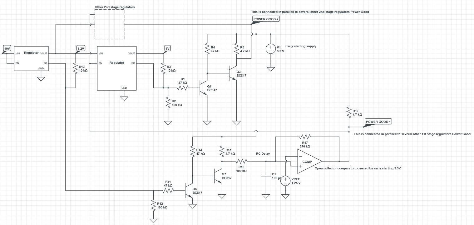
I have setup a primitive sequencing scheme with RC-delays and comparators which turns on the regulators in order. The problem here is I need to monitor several Power Good pins which are tied together.

As I understand it the Power Good pins are open drain pins which are pulled to ground if VOUT of the regulator is below (or over) a certain level. Unfortunately (and obviously) they don't pull to ground if there is no input voltage present at the regulator input. So the input to the comparator needs to be pulled up, possible to parallell and only assert when all Power Good pins are OK.

My current idea of solving this is the below transistor circuit: When the first regulator turns on, its VOUT pulls the PG pin which should be low until VOUT is OK. The transistors connected to the PG pin are set up so they ground the line which is paralleled to other regulators PG during the startup, and releases the global PG only when the regulator PG is OK. When all Power Goods are released this will trigger the enable pins of the next stage of regulators.

Will it work?
enter image description here

schematic

simulate this circuit – Schematic created using CircuitLab

\$\endgroup\$
10
  • 1
    \$\begingroup\$ Is it only my browser or is it almost impossible to see what's on the schematic? \$\endgroup\$
    – Dejvid_no1
    Commented Sep 13, 2016 at 21:03
  • 1
    \$\begingroup\$ its only your browser, for me its not almost impossible, its totally impossible. \$\endgroup\$
    – PlasmaHH
    Commented Sep 13, 2016 at 21:22
  • \$\begingroup\$ :( Tried it in Explorer with the same crappy results. But it is at least possible to open it via the "Simulate this circuit" link. \$\endgroup\$
    – Dejvid_no1
    Commented Sep 13, 2016 at 21:26
  • 1
    \$\begingroup\$ you might be able to condense the layout a bit so everything gets bigger, relatively. \$\endgroup\$
    – PlasmaHH
    Commented Sep 13, 2016 at 21:27
  • 1
    \$\begingroup\$ Looks like it should work. Consider adding something to discharge C1 quickly when main power is off. The simplest would be a diode from C1 to 3.3V. \$\endgroup\$
    – rioraxe
    Commented Sep 14, 2016 at 0:29

1 Answer 1

1
\$\begingroup\$

Rather than build your own discrete solution out of transistors, I'd highly recommend using a reset / supervisor IC for this. I used that approach when I had to solve this exact same problem on a design in the past. They do the exact job you're trying to do here -- wait for voltage to stabilize, then release the /RESET signal after a fixed amount of time. Just hook that supervisor IC up to the regulator's output, and use its /RESET output as the ENABLE input to the downstream regulator.

They're tiny and cheap -- I'll wager a smaller and cheaper solution than a discrete circuit. A few examples:

Some SOT-23s from ST

TPS3836 from TI

\$\endgroup\$

Your Answer

By clicking “Post Your Answer”, you agree to our terms of service and acknowledge you have read our privacy policy.

Not the answer you're looking for? Browse other questions tagged or ask your own question.