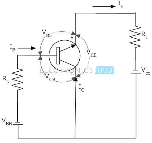
The common terminal of the transistor configuration is also the GND of the circuit, right? I get it that emitter is GND but how is it possible for NPN transistor that base or collector is GND?
2 Answers
The expressions "common (terminal)" are confusing. It refers to the terminal that doesn't carry a signal, so it's considered common to both the input and output. It's not necessarily ground. In the circuit of your diagram the input is the base and the output is the emitter, so it's called a common collector. That particular configuration is more commonly called an "emitter follower," BTW.
-
\$\begingroup\$ If I understood you correctly: CE has emitter grounded by both input and output, when talking about CC, the collector is not used by either of input or output and for CB is the same as for CC except the base is put instead of collector. Am I right? Could this be simple but well defined answer to "What means common in each configuration" ? \$\endgroup\$ Commented Dec 13, 2016 at 19:54
A transistor has three terminals. An abstract "input-output" box has two ports -- an input port with two terminals and an output port with two terminals. That's four, altogether.
One terminal of the input can be connected to one terminal on the transistor. One terminal of the output can be connected to one other terminal on the transistor. This leaves one transistor terminal for the two remaining port terminals. Whichever transistor terminal gets tied both ways -- to a terminal on the input and to a terminal on the output -- is the "common" terminal of the transistor.
This means there are common collector, common emitter, and common base possibilities. And that's all there are.
All of the above has nothing whatever to do with the determination of a node called "ground," which might not even be ANY of the terminals under consideration. You might have a transistor in some odd-ball corner of a circuit and it STILL will have to be operating in one of those three arrangements if it is being used as an input-output port device and it STILL will have none of the terminals at GND. The one idea has nothing necessarily to do with the other. It's just a coincidence that it is often much easier for a designer to arrange their signalling so that it's single-ended and there is a "common" bus, so to speak, for the circuit and that doing so can also help simplify solving equations.
Also, your schematic doesn't show a GND node, anyway. So far as I can tell, it's part of some other circuit that has GND at some other node not shown there.
But by inspection you can easily see that the collector is "common."
Here's an experiment for you. Take your diagram and turn it upside down and look at it, then. Also, feel free to select ANY of the terminals and label it GND (so long as you don't label any of the others GND at the same time, of course -- just one.) None of that changes the operation. But perhaps it will change your perspective.
-
\$\begingroup\$ CE has emitter grounded by both input and output, when talking about CC, the collector is not used by either of input or output and for CB is the same as for CC except the base is put instead of collector. Am I right? \$\endgroup\$ Commented Dec 14, 2016 at 16:42
-
\$\begingroup\$ When talking about Ebers-Moll model of transistor, the common terminal is always grounded, but when talking about normal transistor circuit scheme CE has emitter grounded while other two CC and CB don't have common terminals directly to GND. \$\endgroup\$ Commented Dec 14, 2016 at 16:45

