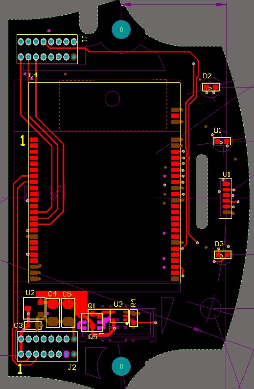
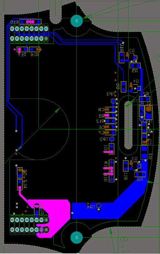
I'm using 4 layers PCB, with the following stuck-up:
Signal1 GND VCC Signal2
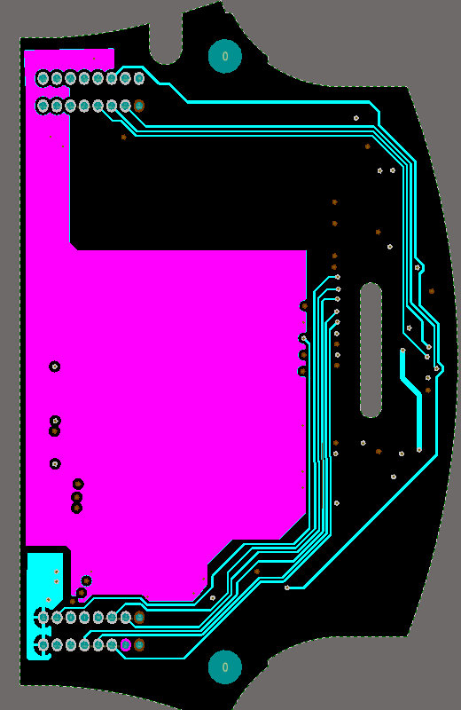
the GND layer flooded with GND Not all the VCC layer flooded with VCC because I needed to route some nets there
I've some free spaces on layer 2&3&4... What should I do with it?
To flood with GND any free space? or can I just leave it without flooding...


