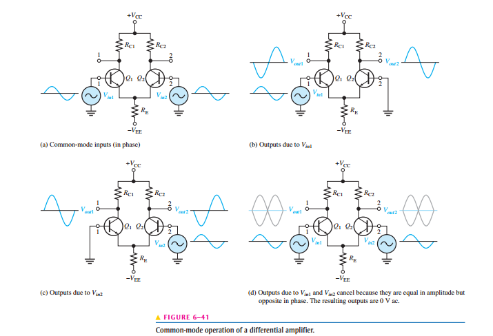
The first approach :Assuming 0v at both bases, when the base input of Q1 rises, its collector current rises and its collector voltage goes down. When the base input voltage of Q2 rises by the same amount, the same happens and its collector voltage also goes down,so the voltage difference between the two collector voltages will be zero.
The second approach : the same thing happens as the first approach but each emitter of both transistors acts like an input to the other and each transistor acts like a common base amplifier and the collector voltage will be in phase with emitter of the same transistor, and out of phase with the amplified signal from its base so they will cancel and the voltage of any collector to ground will be 0v.
I think i confused you a little but here's a photo from "electronic devices" by floyd to make the second approach clear.
I know i got something wrong -as usual- but i want to know where.

