5
\$\begingroup\$

I occasionally like to try to understand how well-known integrated circuits work by building them up in a simulator and observing how they respond to changing conditions. However, I keep coming across multiple-collector or multiple-emitter BJTs, and the simulator I like to use (the one at http://www.falstad.com/circuit) does not have any model for such a device. While I am sure they can be found as SPICE models, for the sort of intuitive understanding I am trying to develop, SPICE simulations simply don't help much, as they don't permit live editing. So my question is this:

How can one best simulate multiple-collector/emitter BJTs without having a simple model for them? Can you use, for example, two BJTs with connected collector and base to simulate a two-emitter transistor? Or would that not work the same? Note that, as this is for simulation purposes only, device mismatches need not be considered.

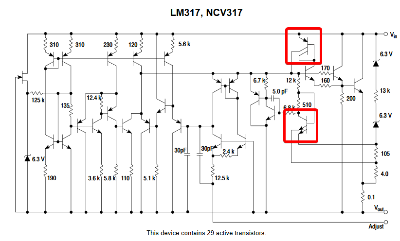
For an example of the sort of circuit in question, LM317 equivalent circuit

This is the equivalent circuit given in ON Semiconductors' datasheet for the LM317 linear regulator. It contains one two-emitter transistor and one two-collector transistor; the latter seems to be just a current mirror, but the function of the former is less clear.

\$\endgroup\$

1 Answer 1

4
\$\begingroup\$

I'm a hobbyist. So keep in mind my own limitations as I write here. And it may have helped me (or others) if you'd provided a specific schematic to discuss. (Update: thanks for adding a schematic!)

Some broad thoughts:

  • The multiple emitters are buried inside of a single BJT structure's base and collector regions, without creating any separating metalization. If you took two BJTs and tied them together in some fashion, all you can do is connect two bases together through the metalization and wiring (same for the collectors), and this is not the same thing as being able to bury emitters directly inside a single structure (just as you can't make a BJT out of wiring two diodes together.) You can't exactly "get there from here," so to speak. More on this, later.
  • The areas can be designed to be different, leading to different parameter values (\$I_{SE}\$, for example) for each. You'd need to study the circuit to see if that feature was being used. If so, you'd need to fashion different BJT models for your simulation and you'd need to understand the schematic pretty well to make reasoned judgments here. Of course, even then it's not exactly the same thing.

In logic circuits, you can usually "get by" with a pair of BJTs, connecting the bases together and the collectors together -- given modest care. With analog, I'd be very wary and worry a lot about the design details, though.

So while I don't think you can directly simulate them with precision from DC to daylight without very specific design information out of which you might be able to design a well-considered subcircuit, you usually can read the schematic and work out a way to provide approximate simulation. (Given the caveat that the more effort you can apply to studying the schematic's design, the better the resulting simulation will be.)


Sidebar: During turn-on, emitter crowding is a significant problem and its effect is magnified by the RC time constant created by the base resistance and the junction's capacitance; with the edges turning on faster than the center of the emitter. Given that the ratio of the perimeter to the area varies with the exact details of the design, this crowding issue also varies too with design details. To reduce the problem, the width of the emitter must be narrow. Sometimes, specialized BJT designs will include multiple emitters in the design in order to maintain DC current drive capabilities while at the same time reducing the AC/transient crowding.


I believe when facing logic circuits you can usually finesse these issues and set up a reasonably well-working arrangement with simple, discrete BJTs (and, possibly in some cases, with some well-placed, added resistors.) You may want to adjust some of the BJT parameters, such as \$I_{SE}\$ and/or \$I_S\$. But without any detailed information to go on, it would all just be guess-work. So I probably wouldn't bother too much there.
\$\endgroup\$
5
  • \$\begingroup\$ Thank you! I've added a schematic as you suggested, but it seems it is, as I feared, not feasible to do. If I'm reading your answer correctly, I think it would require an understanding of the circuit's operation, and given that the entire reason I do these simulations is to help get a better understanding of the circuit's operation, it's kind of a catch-22. \$\endgroup\$
    – Hearth
    Commented Apr 21, 2017 at 23:10
  • \$\begingroup\$ @Felthry The default assumption here would be that the collector current densities are the same and that you can use a simple BJT pair to set this up. But it's hard to know it's exact design intentions without spending more time on the schematic itself. They may have arranged things in the actual design so that the gain is a lot less than one, for example. In that case, you'd replace the diode-connected BJT with an actual diode (and the right parameters.) \$\endgroup\$
    – jonk
    Commented Apr 21, 2017 at 23:26
  • \$\begingroup\$ @Felthry So yeah. You are right in saying that it requires an understanding of various electronics design topologies to have a good chance at arranging an accurate spice simulation. And if an accurate spice simulation is needed for you to understand the topologies, then you are indeed in a catch-22. The way to break out of that is to ask the question like this: "What kind of topology is this LM317 element here? I'd like to study how it works, but I don't know what it is called." That may get specific help, one step at a time, and break the catch-22 cycle. \$\endgroup\$
    – jonk
    Commented Apr 21, 2017 at 23:30
  • \$\begingroup\$ @Felthry This comment should have been first. But I had to delete and re-add it here: The pair in the upper right corner of your schematic is a current mirror pair and it's NOT a multiple-emitter arrangement, but now a multiple-collector one. So my comments above are far less applicable to this case. \$\endgroup\$
    – jonk
    Commented Apr 21, 2017 at 23:47
  • \$\begingroup\$ Suggestion: first assume the multiple-emitter devices split the current equally, and think through (or simulate) the circuit behavior. Some of these are very imbalanced, to create tiny tail currents for the input diffpairs of opamps. As jonk says "it could be guesswork". Unless you want to reverse engineer the circuit, just have fun learning the functioning. \$\endgroup\$ Commented Apr 22, 2017 at 3:36

Your Answer

By clicking “Post Your Answer”, you agree to our terms of service and acknowledge you have read our privacy policy.

Not the answer you're looking for? Browse other questions tagged or ask your own question.