3
\$\begingroup\$

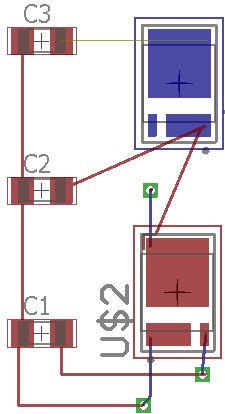
I defined a device (MOSFET) using the schematic and package from other components and placed 4 in my schematic. When trying to route connections, these parts can only be interconnected using bottom traces even though they were placed and appear as top layer components (red, not blue). If I mirror the component, it turns blue and I can connect top traces (red) to the blue component.

What have I done wrong that would make this happen?

The photo shows this

\$\endgroup\$
3
  • 1
    \$\begingroup\$ Could you upload your .brd file to here \$\endgroup\$ Commented May 29, 2017 at 19:02
  • 1
    \$\begingroup\$ While unrelated to your difficulty, you probably want much wider traces if you plan to leverage what FETs in a package like that are capable of. \$\endgroup\$ Commented May 29, 2017 at 19:54
  • \$\begingroup\$ Wires are drawn manually; top airwire does not go to center as @DaveTweed noticed because it was wire before, then got deleted, but airwire in the shape remains. For me question is absolutely unclear, what and how was done unclear, so we may be troubleshooting issue which does not exist. That's why I initially came with answer for OP to at least get some info how to use EAGLE so that we can be sure he follows the rules. \$\endgroup\$
    – Anonymous
    Commented May 29, 2017 at 20:55

2 Answers 2

-2
\$\begingroup\$

There's an issue with self-created library part; some component was used as a source (e.g. DPACK), and then polygons were drawn over the pads instead of reshaping the pads. If EAGLE EDA tool is used properly there will be no such issues like this.

So: seems you need EAGLE basic tutorial, start with this one.

There're some rules how you create board layout, and how you route the board. Red means surface of the board you look at, "blue" means surface of the board at the other side. They are called top and bottom respectively.

You can not connect top and bottom components properly without vias.

Polygons are tricky elements, I do not remember I used them at the device level. Wires do connect pads, not polygons.

In your picture you actually did not connect "red" to "blue", you put red traces at the top of the board towards the place where bottom component's pad is located. There's a tool called DRC (design rule check), and running it you will see errors for your current drawing.

I think in your situation you can try autorouter (if you have a licence for it), and you will see how it routes. At least you will have an idea how your board may look like. Then, go to examples directory and examine example projects to see how they are made.

P.S. Thanks every one participating in the discussion :)

\$\endgroup\$
7
  • \$\begingroup\$ You seem to have misunderstood the issue. The poster is quite clear that the tool is only allowing connections to what is seemingly the "wrong" side of the shown pads. The fact that it is not connecting the traces to the center of those pads may well be a clue to what is actually being connected, but you have failed to in any way address the actual difficulty of why it is not permitting connection to the pads on the surface on which they appear, but only permitting these odd connections. \$\endgroup\$ Commented May 29, 2017 at 18:58
  • \$\begingroup\$ @ChrisStratton undeleted this answer because I am sure that OP just did not follow the rules using EAGLE drawing his board, and he needs initial basic EAGLE training. \$\endgroup\$
    – Anonymous
    Commented May 29, 2017 at 21:02
  • 3
    \$\begingroup\$ The problem is far too consistent to be a simple user error in manual routing as you allege. It's likely there's a problem with the self-created library part. There's already been a request for the actual board file which would contain the part definition to analyze; the smart thing to do when a question is unclear is to use a comment to ask for sufficient information and then wait for a response. \$\endgroup\$ Commented May 29, 2017 at 21:07
  • \$\begingroup\$ @ChrisStratton I would agree that there's an issue with self-created library part; some component was used as a source (e.g. DPACK), and then polygons were drawn over the pads instead of reshaping the pads. Again, if tool is used properly there will be no such issues like this. \$\endgroup\$
    – Anonymous
    Commented May 29, 2017 at 21:55
  • \$\begingroup\$ @Anonymous It appears the creator of the package used polygons instead of modifying the pads. It will likely be easier to create a new package than debug the previously defined package, so I will try that. I had spent 2 days searching and trying things before you provided the most likely cause of the problem! Thank you very much! \$\endgroup\$ Commented May 30, 2017 at 1:11
-1
\$\begingroup\$

Mirroring parts is equivalent to flipping them to the bottom layer. Mirror again to flip it back to the top layer.

The traces arent actually connected to the bottom pad. The airwires are not visible because they're going "straight down."

\$\endgroup\$
5
  • \$\begingroup\$ No, something else is wrong. The airwires are not even going to the centers of the "pads" -- note the one at the top connected to C3. Something is really messed up here, but I can't imagine what it might be. \$\endgroup\$
    – Dave Tweed
    Commented May 29, 2017 at 20:06
  • \$\begingroup\$ @DaveTweed C3 airwire was manually routed wire before, then was deleted, but the shape remains. \$\endgroup\$
    – Anonymous
    Commented May 29, 2017 at 21:00
  • 1
    \$\begingroup\$ @Anonymous that fails to explain why the one visible air wire matches the extremely consistent endpoint of each trace in the wrong place on the wrong side of the board. Clearly the tool wants to connect them in those places; the question is why. \$\endgroup\$ Commented May 29, 2017 at 21:11
  • \$\begingroup\$ @ChrisStratton Because actual device's pads are covered by the polygons/rectangles drawn at the package level in library editor. Most probably source package used was DPACK. \$\endgroup\$
    – Anonymous
    Commented May 29, 2017 at 21:53
  • \$\begingroup\$ Anonymous: There must be polygons defined for the FET to sit on for cooling. One polygon also covers the 4 drain pins that are common. Another polygon covers the 3 common source pins. DRC complains there is overlap, but I assumed that was an acceptable error since the objective is correct. Maybe Eagle is preventing a connection on the top layer because the polygon does not have the same net name as the pins, which would also explain the OVERLAP error. This is a test to show a much simplified version of the problem. So, traces will be wide, two-sided with lots of vias, 3 oz. copper, etc. \$\endgroup\$ Commented May 30, 2017 at 0:02

Your Answer

By clicking “Post Your Answer”, you agree to our terms of service and acknowledge you have read our privacy policy.

Not the answer you're looking for? Browse other questions tagged or ask your own question.