0
\$\begingroup\$

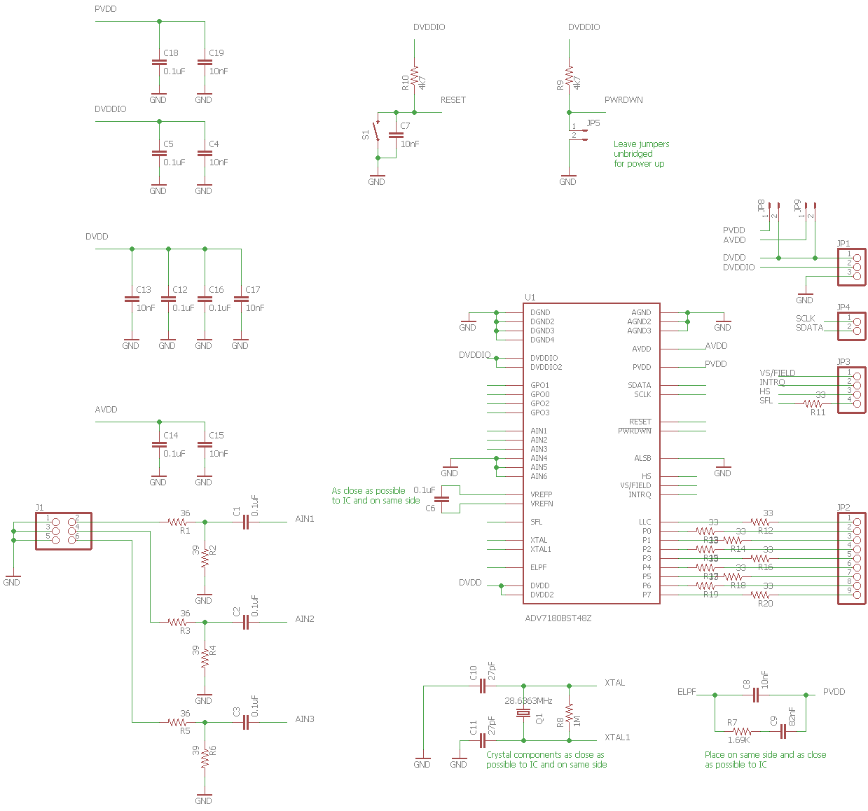
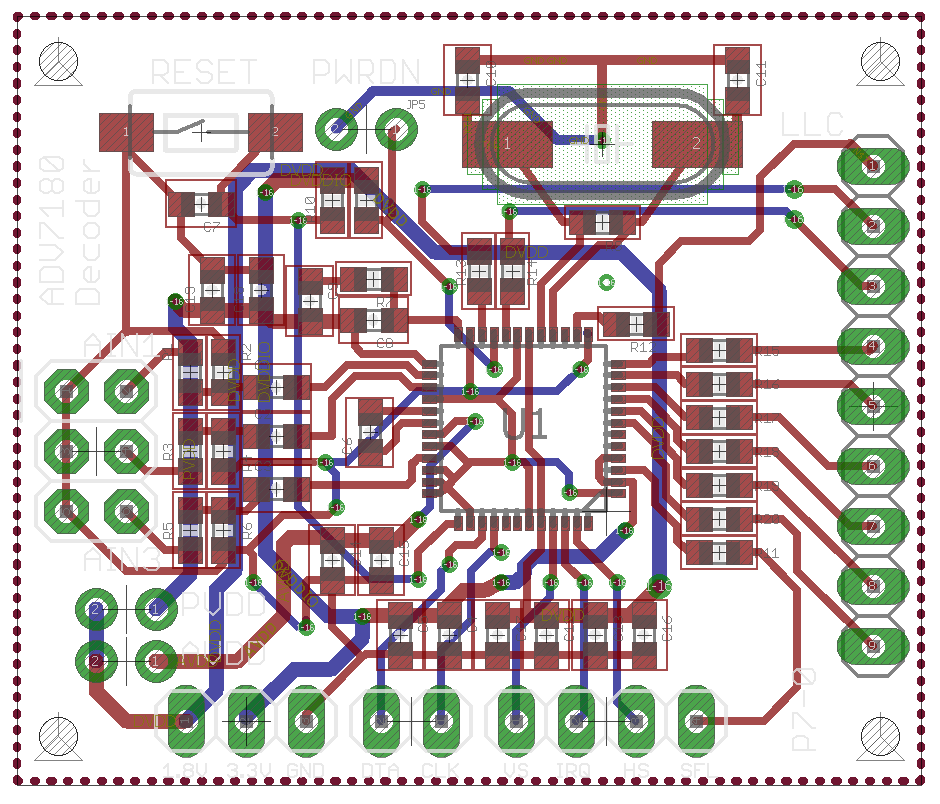
I plan to make a breakout board for Analog Devices's ADV7180 analogue video decoder IC. I wonder if someone would be kind enough to look over my schematic and board layout and let me know if I'm making any basic mistakes before I attempt to have the board made. Ultimately I hope to connect this to an FPGA and do some image processing before connecting to another breakout board with an ADV7391 encoder.

Board layout Schematic

Some of the questions I'm uncertain about:

  1. This device has a 27 MHz data clock and parallel port. Can I use 2.54 mm pinheaders or do I need something more suited to high speed data?
  2. Is it safe to route the clock line over 2 data lines as I have done or do I need to take those 2 lines right up and around?
  3. Where there are multiple pins for one supply do I need decoupling capacitors on each pin or is it OK to have decoupling capacitors on one pin then a trace to the other pin?

Any comments or feedback will be much appreciated.

\$\endgroup\$
1
  • \$\begingroup\$ Having used this family of devices in avionics, C0G devices are highly recommended for the PLL loop filter, as class 2 dielectrics have too much drift over temperature for stable operation. \$\endgroup\$ Commented Jun 17, 2017 at 13:31

2 Answers 2

2
\$\begingroup\$

10-bit ADC running at 57-86 MHz according to datasheet?...

There is no way in hell this will work without a solid ground plane. Also, a look at how the decoupling caps are laid out makes me believe you are inexperienced in this kind of highspeed layout. I mean, it's not a crime, OK? But please don't send this to the pcb fabrication, it will only result in massive headaches when you try to make it work. Let's try to save you the pain shall we?

You can get 4 layer protos for $50 these days, which means as a hobbyist, it is not worth spending a weekend hours making a perfect 2-layer layout...

This device has a 27 MHz data clock and parallel port. Can I use 2.54 mm pinheaders or do I need something more suited to high speed data?

2.54mm headers are perfectly fine provided you got enough ground pins, ideally one between each highspeed signal, but this looks like it's not the case, so expect some signal integrity issues. With resistors to slow down the signals, it should work, but you could lose a few LSBs to noise.

Is it safe to route the clock line over 2 data lines as I have done or do I need to take those 2 lines right up and around?

Nope, use a 4 layer board and do it right.

Where there are multiple pins for one supply do I need decoupling capacitors on each pin

Yes, the purpose is low inductance, so you need those caps.

Reminder: if you use 0805 caps, they all have the same inductance regardless of value, so get the largest value you can like 10µF.

I posted this on decoupling.

OK, so advice:

  • I just checked on seeed and pcbway: 4 layer is $50 no matter the size, up to 10x10cm, so DO NOT MAKE YOUR PCB THAT SMALL!
  • Add test points for your probes,
  • Do the encoder and decoder on the same board
  • If you want to input your video signals using BNC or RCA connectors, then get the cheap PCB-mounted ones. DO NOT put 3 video signals on a 0.1" header with 1 GND pin, they will crosstalk. Stick 3 pcb-mount coax connectors on your ground-plane PCB.

EDIT:

Coolrunner 2 is a CPLD, not a FPGA. Make sure you're familiar with the differences. Doing a layout for a FPGA board is rather complex, and as an amateur you will be restricted to the ones in "not BGA" packages. I would strongly advise using an off the shelf FPGA board, there are good ones, packed with features, at affordable prices.

If you make modules with connectors, make sure they're compatible! This kind of requires choosing the FPGA board first.

Now if you want a FPGA and a micro on the same board, your choices will be more restricted of course. Or you could get something like a Zynq board. It's overkill, but well, you get a FPGA, an overpowered Cortex-A9, and a bazillion peripherals for $99... not worth rolling your own at this price! Focus on your real project goals, not building tools that you can buy off the shelf at very reasonable prices...

3.3V and 1.8V are supplied by a separate board with LDO voltage regulators powered by a USB connector.

Aw, come on, put the LDOs on the same board, they use little space and it's hard to get wrong.

The FPGA does not need to do any sophisticated DSP, only read the RGBA for the current/next pixel from the frame buffer, use them to perform some simple math on the current pixel value from the ADV7180 as it comes along the wire, then pass the updated value to the ADV7391. And arbitrate between itself and the microcontroller, which needs to be able to update the frame buffer.

Maybe you could do that with an XMOS too, if you're not fond of HDLs. Or an ARM SBC with a USB video acquisition dongle...

\$\endgroup\$
10
  • \$\begingroup\$ Thanks for your feedback. I have made a few DIY circuit boards but not with this level of complexity. It is starting to look as if this project is more worthy of a grad student than a hobbyist. \$\endgroup\$
    – Batperson
    Commented Jun 18, 2017 at 10:01
  • \$\begingroup\$ Assuming I do go ahead with it, am I reading you right that a 4-layer board is a requirement with this type of circuit, or is 2-layers doable? Does a copper pour connected to ground on the bottom layer count as a "good solid ground plane?" \$\endgroup\$
    – Batperson
    Commented Jun 18, 2017 at 10:11
  • \$\begingroup\$ Although the device has 3 inputs for 3 video signals I'm only intending to use 1 at a time (1 CVBS signal), although if I got as far as a working circuit I might try switching between inputs. \$\endgroup\$
    – Batperson
    Commented Jun 18, 2017 at 10:15
  • \$\begingroup\$ Well, in a realistic system this chip would sit next to a CPU/DSP or other digital video processing chip, probably a BGA one, with RAM chips... all this needs a multilayer board too. And 4 layers with continuous ground plane will give a massive boost to your chances of success ;) Copper pour won't cut it unless it is continuous. I don't see 1.8V LDO in your schematic, where does the 1V8 come from? Also what FPGA board are you using? \$\endgroup\$
    – bobflux
    Commented Jun 18, 2017 at 11:33
  • \$\begingroup\$ 3.3V and 1.8V are supplied by a separate board with LDO voltage regulators powered by a USB connector. My plan was to put everything on separate boards, that way I could get everything working individually before connecting them up. \$\endgroup\$
    – Batperson
    Commented Jun 18, 2017 at 21:32
0
\$\begingroup\$

For readabillity I would suggest using less labels, I personally especially with these small pcb's try to minimize the use of labels as much as possible it is a hassle to search where all the signals are going and as long as your schematic isnt covering multiple pages there really isn't a use for it.

@peufeu already gave some good advices,

I would add the following stuff.

1) If you are using the BNC connectors (try to make the pcb trace 50 ohm impedant just like the BNC connectors usually are. This prevents reflections.

2) Leaving Reset and Powerdowns pins floating, can be tricky. I have personally experienced this not giving the desired result even though the datasheet mentions you can leave the pin open, I would suggest you just tie it to GND or VCC dependent on whatever you want to do with it.

3) I personally always design PCB's with a look into the future, if you are gonna produce it why not just make pads and stuff for a external crystal. You dont have to use it. But at least you will have the option in the future if it turns out to be useful

\$\endgroup\$
4
  • \$\begingroup\$ Thanks, I will take onboard your suggestion on readability. Reset and Powerdown are not floating, they are connected to VDDIO with a button to pull reset low, and a jumper to do the same for powerdown. There is an external crystal. \$\endgroup\$
    – Batperson
    Commented Jun 18, 2017 at 9:58
  • \$\begingroup\$ Oh yes I see now, well that's what I meant with readabillity haha, If you're using labels like you are at least also apply them at the microcontroller, I didn't see it was connected. Same goes for the crystal, but I was tired as well haha ;) \$\endgroup\$
    – Remco Vink
    Commented Jun 18, 2017 at 12:18
  • \$\begingroup\$ There is no microcontroller ;-) But you are right, most of the nets are unlabelled. They are labelled at the pins but it is not obvious that they are connected to anything I guess. \$\endgroup\$
    – Batperson
    Commented Jun 18, 2017 at 21:26
  • \$\begingroup\$ IC ;), i should get more sleep or more coffee. Apologies \$\endgroup\$
    – Remco Vink
    Commented Jun 19, 2017 at 5:36

Your Answer

By clicking “Post Your Answer”, you agree to our terms of service and acknowledge you have read our privacy policy.

Not the answer you're looking for? Browse other questions tagged or ask your own question.