1
\$\begingroup\$

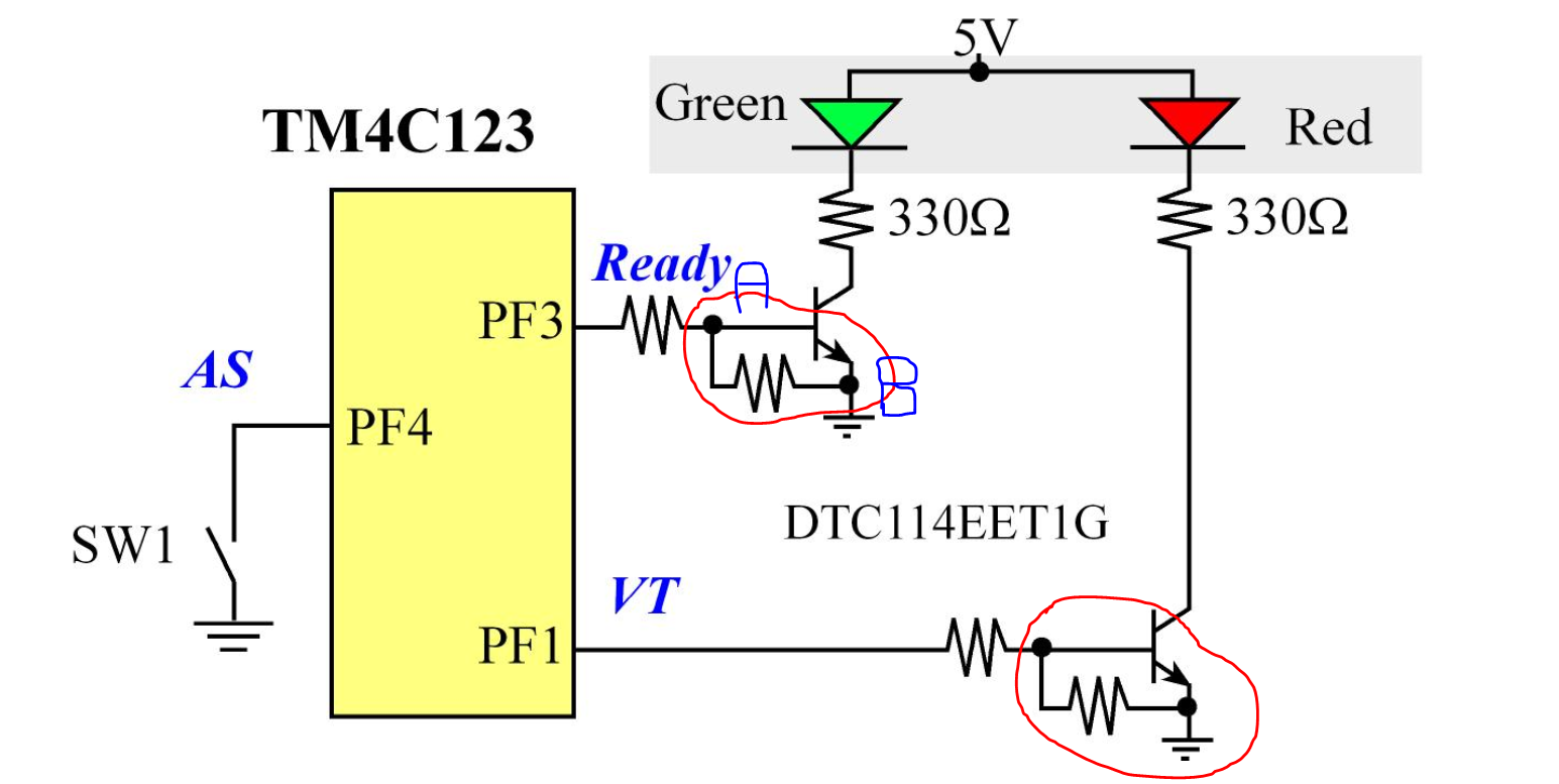
I have a diagram that represents a circuit whose purpose is enabling/disabling two leds basing on a logic programmed in a micro-controller.

In the circuit below, as far as I understand, there are two n-type transistors, and they have a resistor connecting their gates with their sources, respectively.

enter image description here

My questions is: Why are the marked resistors necessary? (red circle)

\$\endgroup\$
3
  • 1
    \$\begingroup\$ "connecting their gates with their sources" Hi, FYI as shown on the schematic they are BJTs not FETs, so instead of gate & source, those marked resistors are between base and emitter (along with the other resistor in series with the base). \$\endgroup\$
    – SamGibson
    Commented Aug 19, 2018 at 21:18
  • 1
    \$\begingroup\$ Just think of them as Weak pull-downs, the fact they are connected to emitter is does not imply any additional significance, they are pull downs to ground. \$\endgroup\$
    – crasic
    Commented Aug 19, 2018 at 21:23
  • \$\begingroup\$ The base voltage dividers also shift initial switch on input voltage up from 0.6V. This can be used to move switching point towards midway input voltage swing dramatically improving noise margin \$\endgroup\$
    – carloc
    Commented Aug 20, 2018 at 7:37

5 Answers 5

3
\$\begingroup\$

When your microcontroller comes up, it's GPIO is in high-Z state, maybe pulled up(that means there is an internal resistor to VCC which may be enough to turn on the LED) . Its a good practice to pull down anything you don't want to work uncontrolled. So when the firmware initializes the outputs, you don't need the pull down resistors anymore. Only on power up/down or JTAG programming.

\$\endgroup\$
1
\$\begingroup\$

The resistors to ground aren't necessary. However, you can get "logic transistors" that contain all of those resistors plus the actual transistor in a single package, which is probably why they're in the circuit. (It saves one component on the board.)

\$\endgroup\$
1
  • 1
    \$\begingroup\$ You're right, that schematic is showing "logic transistors" (the manufacturer calls them BRT - Bias Resistor Transistors). Here is the relevant datasheet, in case it's helpful to readers: DTC114EE \$\endgroup\$
    – SamGibson
    Commented Aug 19, 2018 at 21:23
0
\$\begingroup\$

That is a voltage divider hybridized with a current limiting resistor. It seems to me an odd way of doing it though. I am guessing because it keeps from adding more resistance to the collector circuit?

\$\endgroup\$
0
\$\begingroup\$

Sometimes the GND voltage at the emitter is not the GND voltage over at the MCU logic level output. This voltage divider provides some noise immunity for that case.

\$\endgroup\$
0
\$\begingroup\$

It's to pull the gate low to make sure it is off when you don't want it on. With a PNP you'd pull the gate high.

\$\endgroup\$
1

Your Answer

By clicking “Post Your Answer”, you agree to our terms of service and acknowledge you have read our privacy policy.