0
\$\begingroup\$

Suppose I have a PCB trace that needs to be impedance matched, but the trace width changes as it travels from its source to its destination. Something like this: Trace width change

The 5mil trace would have a certain characteristic impedance, whereas the 10mil trace would have another impedance. How do these two different impedances combine? Asked differently, what is the equivalent impedance of this trace?

\$\endgroup\$
8
  • 2
    \$\begingroup\$ There is no "equivalent impedance", the characteristic impedance is a local property of a transmission line. You will have jumps in impedance and corresponding signal reflections if the length of these uneven sections is comparable with wavelength of transmitted signals. \$\endgroup\$ Commented Oct 25, 2018 at 17:18
  • 1
    \$\begingroup\$ Out of curiosity, why are you doing this? The usual answer is, whatever impedance you want for your trace, pick the width that gives that impedance and stick with it for the whole trace length. Also, if the section that is the "wrong" impedance is very short relative to the wavelength, it can often be ignored. \$\endgroup\$
    – Selvek
    Commented Oct 25, 2018 at 17:31
  • 1
    \$\begingroup\$ While your question is well-formed, it is worth asking before we get into all this, what is your signal, and how long overall is the transmission line? Maybe you don't need to worry about all this. Also, what is the impedance looking into the load? \$\endgroup\$
    – user57037
    Commented Oct 25, 2018 at 17:33
  • 1
    \$\begingroup\$ Well, you will get a reflection from the first point of impedance discontinuity. Then another one from the second point. If the source impedance matches the 5 mil trace impedance, the reflection will be wholly absorbed at the source. If not, it will reflect again. You should DEFINITELY mock this up with spice and observe the signal in the time domain to see what it looks like. This will aid in your intuitive understanding of such things tremendously. \$\endgroup\$
    – user57037
    Commented Oct 25, 2018 at 17:47
  • 2
    \$\begingroup\$ @TRISAbits Given how much time signals spend torturing me, I wouldn't judge anybody for deciding they want to torture their signals :) \$\endgroup\$
    – Selvek
    Commented Oct 25, 2018 at 18:38

3 Answers 3

2
\$\begingroup\$

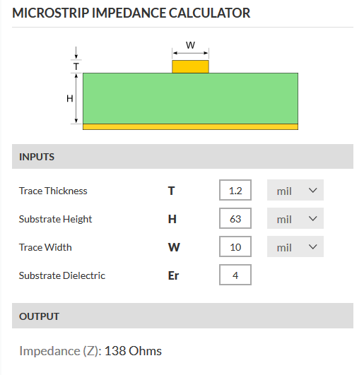
You need to know the height of the trace between the ground plane, the relative electric permeability and how high the trace is to find the equivalent impedance.

For standard FR4 (pcb material) the electric permeability constant is ~4.4. The height will depend on your PCB stackup, and what layer the ground plane is on.

enter image description here

enter image description here
Source: https://www.eeweb.com/tools/microstrip-impedance

If the transmission lines are not matched, you will get a reflection at the point of mismatch and lose power.

The equation for finding this would be the reflection equation:

Z1 would be the characteristic impedance of the 5mil trace, and Z2 would be the impedance for the 10mil trace (after you calculate it)

enter image description here

\$\endgroup\$
2
  • 1
    \$\begingroup\$ Your right, I'll edit it \$\endgroup\$
    – Voltage Spike
    Commented Oct 25, 2018 at 17:18
  • 2
    \$\begingroup\$ There is a rule of thumb that the 50 Ohm trace width is around W = 2H. Very useful when doing feasibility checks and sanity checks. The effect of changes in T is relatively minor most of the time. \$\endgroup\$
    – user57037
    Commented Oct 25, 2018 at 17:42
1
\$\begingroup\$

Assuming the height above the ground plane is the same for the whole trace, the 5-mil-wide segments will have one characteristic impedance and the 10-mil-wide segment will have a different, lower, characteristic impedance.

The whole trace would not normally be thought of as having a single "equivalent impedance" characteristic.

What you could do is calculate the input impedance, or the S-parameters of the trace, as a function of frequency. To do this, you could use a simulation tool like Keysight ADS, or Smith chart techniques (if you are only interested in the input reflections), or simply sit down and do a bunch of algebra.

\$\endgroup\$
3
  • \$\begingroup\$ Do you of a place where I can find the math to do this by hand? \$\endgroup\$
    – TRISAbits
    Commented Oct 25, 2018 at 17:23
  • 1
    \$\begingroup\$ @TRISAbits, it should be in any E&M textbook, like Ramo, Whinnery, and Van Duzer, for example.Or on Wikipedia. \$\endgroup\$
    – The Photon
    Commented Oct 25, 2018 at 17:26
  • 1
    \$\begingroup\$ You need to (at a minimum) model this as three transmission lines. The 50 Ohm segment (5mils), the 25 Ohm segment (10 mils) followed by another 50 Ohm segment. You will need accurate models for the input impedance of the load and the output impedance of the source. Ideally, you would use simulation software capable of modeling PCB layouts. I am just guessing on the Ohms. You should use calculated values. \$\endgroup\$
    – user57037
    Commented Oct 25, 2018 at 17:38
1
\$\begingroup\$

I fear you have entirely missed the point of controlled impedance. Your diagram actually looks (from an impedance point of view) like this

schematic

simulate this circuit – Schematic created using CircuitLab

where Z0 and Z2 are 5 mil lines, and Z1 is your 10 mil line.

The whole point of using a controlled impedance line is to ensure that the junction of Z2 and ZLOAD does not cause a reflection when the signal hits it. Assuming that, with your board geometry and material properly selected, Z2 and ZLOAD are in fact matched, you now need to consider the rest of the trace.

The junctions of Z0 and Z1, and Z1 and Z2 will BOTH produce reflections, and this is entirely backwards from what you want to do in the first place.

\$\endgroup\$
1
  • \$\begingroup\$ That's a good point. I guess you sort-of could get something like this when a signal changes to another layer, but if you don't respectively match each layer the signal goes across, you don't really have an impedance matched signal in the first place. \$\endgroup\$
    – TRISAbits
    Commented Oct 25, 2018 at 17:45

Your Answer

By clicking “Post Your Answer”, you agree to our terms of service and acknowledge you have read our privacy policy.

Not the answer you're looking for? Browse other questions tagged or ask your own question.