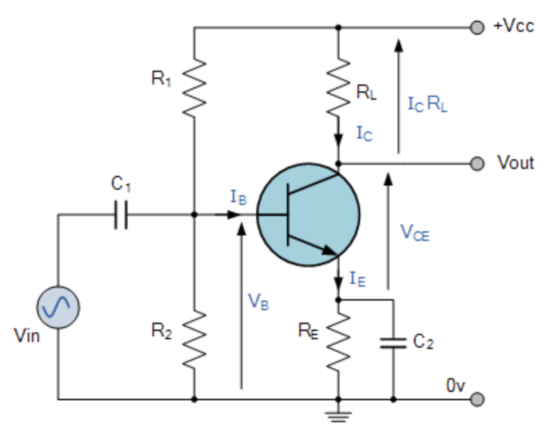
My reasoning is that the whole point of biasing was to prevent
clipping and so biasing the input to half of Vcc would give us maximum
swing.
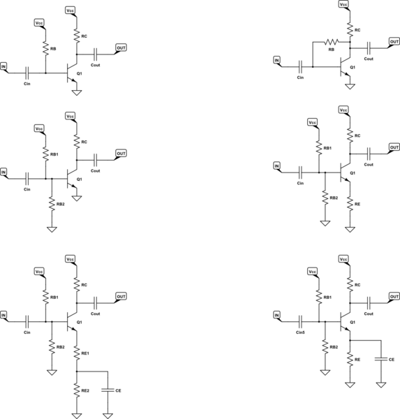
This amplifier arrangement requires some differentiation from other basic CE amplifier topologies using only one BJT. So I may as well list some of them out just to help clarify the situations:

simulate this circuit – Schematic created using CircuitLab
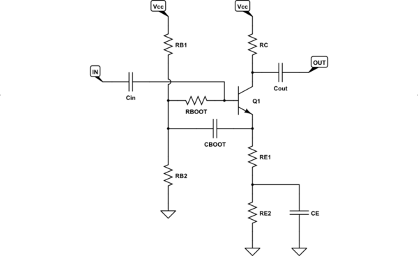
There's more, of course. The above only scratches the surface. For example, here's one with bootstapping to help increase the input impedance:

simulate this circuit
One point I'm trying to get across is that there are myriad topologies for a CE amplifier stage and that there will be varying goals and varying priorities for those goals in designing one or another of the above.
Certainly, if nothing else gets across to you, it should be that either centering the collector voltage between the power rails (or centering the base voltage between the power rails) isn't always going to be the primary (or even an important) goal. If you get nothing else at all, I hope you can at least get this much from just a quick perusal of the above schematics.
So what's important???
- Thermal stability. This can be either stability of the DC biasing point and quiescent current or stability of the AC voltage gain or... well... stability of any desired goal vs temperature. But even that may not be important if global NFB is used to correct the behavior over temperature. So if a specific BJT stage is part of a larger system of stages and there is global NFB operating effectively, then the design of any one specific stage for thermal stability may not be very important, at all. Context matters.
- Input impedance. This can be important (or less so) depending upon the circumstances. The above bootstrapped design was created to improve (increase) the input impedance of the CE amplifier stage. But this may not be a priority if the driving circuit has low impedance. (Also, input impedance can have a thermal component, so see #1 above.)
- Output impedance. Again, this depends upon the context. The output impedance may be important, or not so important. Circumstances matter. (And this can also be affected by temperature.)
- Gain stability vs temperature.
- Gain stability vs signal.
- Gain stability vs output loading.
And there's more, of course. Context matters. You cannot have any hope of prioritizing the above (and other goals) without knowing the full context for the stage. So you need to know what's driving the circuit, what the circuit is itself driving, if there is global NFB operating (and how), and a host of other issues that relate to the design. The available voltage rails also apply in all this, too. So it's important to know how much headroom is available before these factors can be weighed.
Your circuit is an AC-grounded CE amplifier. The emitter resistor's only values are in setting the thermal stability of the DC biasing point and quiescent current and in increasing the input impedance (not because of the emitter side, but because of how it affects the Thevenin of the base biasing pair.) It has no value in improving the thermal stability of the AC voltage gain and won't do much regarding output phase.
In this sense, you'd want to set the base voltage to about midway (discounting base current) between the supply rails because this allows \$R_{\text{B}_1}=R_{\text{B}_2}\$ and maximizes the Thevenin equivalent there. \$R_{\text{E}}\$ is then there to permit that arrangement with its value setting the quiescent DC emitter current (which impacts the AC voltage gain.) Of course, this also means that you would NOT want to set the collector voltage to midway between the supply rails!! So if maximizing the input impedance was more important, you'd sacrifice setting the collector to midway and would move it elsewhere, instead.
With a circuit like this, where \$r_e\$ (which depends upon the collector current at any moment in time) sets a continually signal-varying voltage gain for the circuit, AC gain stability cannot be much of a goal. There must be global NFB operating to deal with that part. So this might actually mean that setting the quiescent collector voltage at about midway between the rails may be a valid goal. However, not exactly midway because you still need to allow for keeping the BJT in active mode (and not saturated.) So this means reserving at least \$1\:\text{V}\$ away from the supply voltage difference. And that means adjusting the quiescent collector voltage at least a little distance away from the midpoint.
If I had to summarize the above with respect to your question, it's almost never a goal to set either the quiescent base voltage or the quiescent collector voltage to midway between the rails. There's always at least some reason to adjust away from that idea. Some ideas would move you further from that; some would get you closer to that. But in all reasonable cases you won't use "midway" as a bright-line decision. There will always be some reason to move at least somewhat away from that simplistic idea.
And note that I haven't even brought up clipping. Of course, that shouldn't happen at all. But handling that aspect is something you do after the other important decisions have been made. You may limit the input range to keep that from happening. Or you may adjust the voltage gain. But regardless of how, it's usually one of the last things you worry about. (A reason to worry about it earlier is if you input specifications provide the exact voltage rails and AC voltage gain and the input signal range and you need to verify that the specified goals are even possible, at all.)
So tell me? How do you think about designing something like your circuit? What do you think is most important? Why?

