1
\$\begingroup\$

I own a set of Soviet IN-14 Nixie tubes and I would like to use them to make a vintage clock. I found this example schematic of a "Nixie clock": Nixie clock schematic
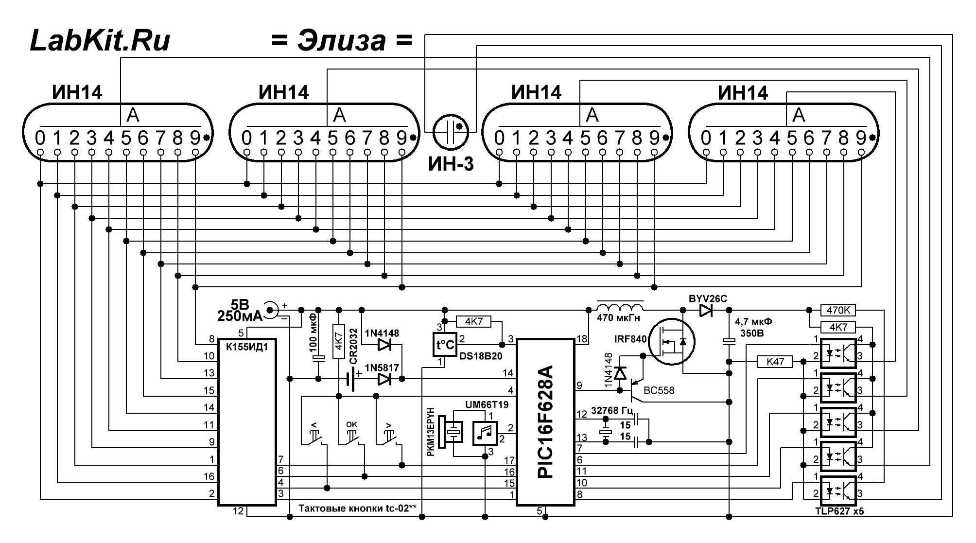
I don't understand what is the purpose of using a MOSFET in the second stage of this quasi-"Darlington pair" (as opposed to a second bipolar transistor in a normal Darlington pair) here: quasi-Darlington pair with a MOSFET
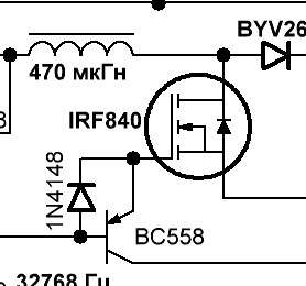
Is there a particular name for this configuration?

As a secondary question, I also would like to know why a diode was used in place of a resistor in this configuration?

\$\endgroup\$
3
  • \$\begingroup\$ @Hearth: This is the answer. \$\endgroup\$
    – Janka
    Commented Jul 7, 2019 at 13:54
  • \$\begingroup\$ @Janka Thanks. Wanted at least one other person to confirm before I made it an actual answer, as I wasn't completely certain that was the whole story. \$\endgroup\$
    – Hearth
    Commented Jul 7, 2019 at 13:58
  • \$\begingroup\$ It is the simple answer without a name \$\endgroup\$
    – D.A.S.
    Commented Jul 7, 2019 at 14:19

2 Answers 2

4
\$\begingroup\$

This is what's called a gate drive circuit, or gate driver. The BC558 aids in pulling charge out of the IRF840's gate, acting as a current amplifier to turn the FET off faster. The circuit designer apparently decided that the turn-on time wasn't as much of a concern, so a 1N4148 diode is used to pass the un-amplified current straight from the PIC's output.

The term gate driver is a generic term, referring to any circuit that aids a signal in charging and/or discharging the gate of a FET or IGBT. I don't think the particular instance in the circuit above has any more specific name.

\$\endgroup\$
1
  • \$\begingroup\$ But why is it done this way is a better Q&A \$\endgroup\$
    – D.A.S.
    Commented Jul 7, 2019 at 17:23
0
\$\begingroup\$
  • it is obviously an active buffered gate driver, but no name yet subtle characteristics.

The IRF has a Vt= 2 to 4 V thus with only 4.4=Vgs to 4.5V the RdsOn is not the same as rated @ Vgs=10V. Due to 5V-0.6 V nom gate drive on 1n4148 for high signal.

  • the nominal curves show Id=1.1 A constant current with no inductor to Vds.

So less than ideal but well damped V=LdI/dt = 2fL I is the boost voltage. (450uH 1.1A x 2 x f) =V yet source is limited by 250mA.

  • The emitter follower reduces the PIC output impedance /10 from 50 Ohms to 0.5 then 5 Ohms when saturated during Ie/Ib=10 to drive Ciss off, thus close to Gate input impedance of 2.8 ohm max.

  • so it is simply slow turn on, fast turn off buffered non-inverting gate drive shunt switch output to gnd with approx a 1.1A current limit for nominal parts at 25’C.

  • Possibly for PFM modulated boost voltage.(TBD determined by timer coding)

The LC resonant Load is 450uH 4.7uF or 3.3kHz so it operates in CCM at higher frequency and select this f determines the desired optimum Tube bias voltage.

p.s. I wonder why to music symbol across the Xtal to PIC.

\$\endgroup\$
1
  • \$\begingroup\$ That's a music player and amplifier IC. I wonder why they did not put a music player into the PIC software. It's simple. \$\endgroup\$
    – Janka
    Commented Jul 7, 2019 at 15:20

Your Answer

By clicking “Post Your Answer”, you agree to our terms of service and acknowledge you have read our privacy policy.

Not the answer you're looking for? Browse other questions tagged or ask your own question.