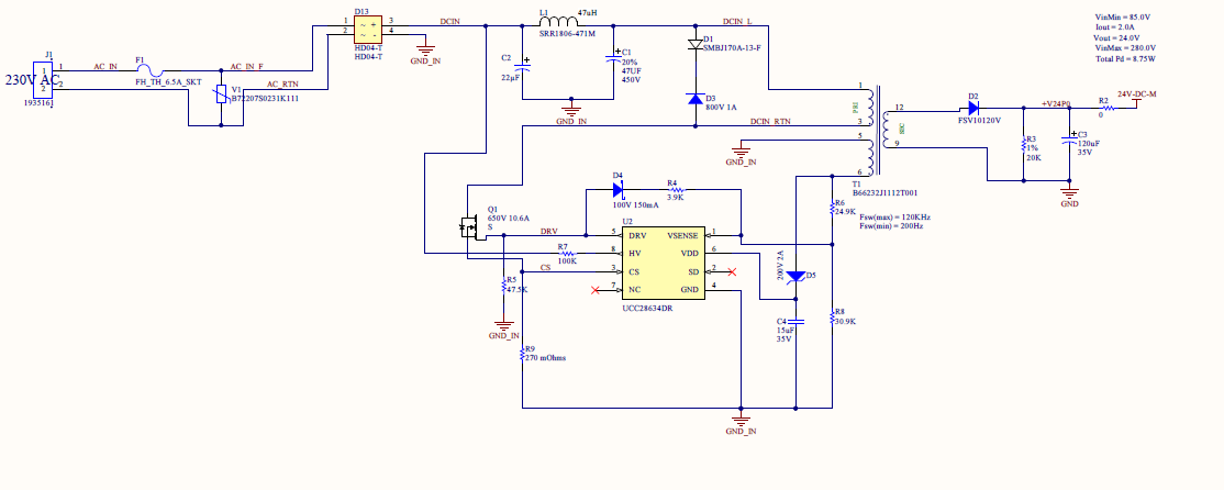
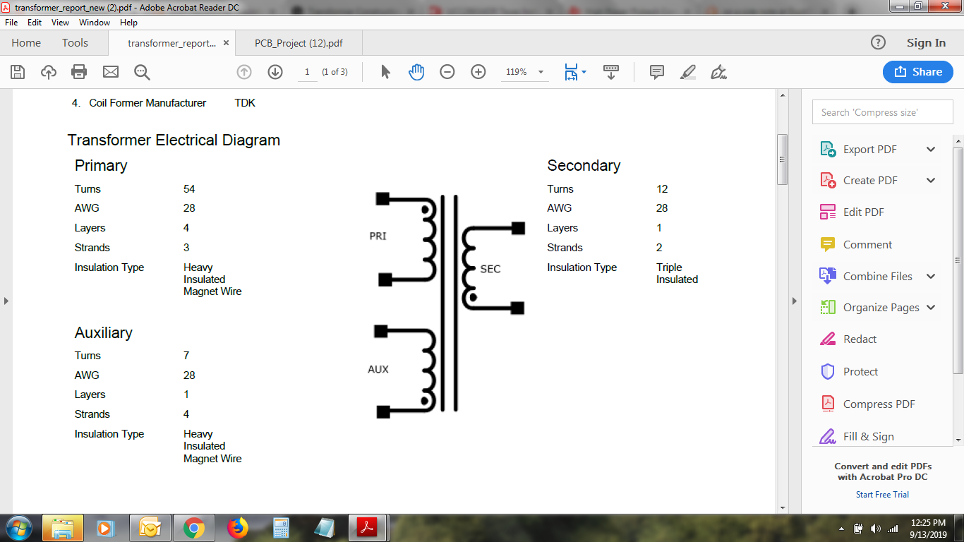
From my preliminary examination, I found that the VDD is fluctuating from 12 to 5v, My inference from the datasheet is that the High voltage current source is helping till it reaches VDD(start) and turns off to let the bias voltage take over, but that's not happening, so it resets, and reinitiates the startup sequence and is in a loop. I'm getting roughly around 300V at the bulk caps after Full bridge rectifier and zero volts at the secondary. Kindly note this is a TI generated schematic. The PWM signals will drive the power Mosfet only when VDD Is at 14.7v. The symbol used in Altium's library for that transformer shows the dot placed wrongly. The transformer used was constructed according to Ti's design report. If someone could help me out on this one it would be greatly appreciated.
-
1\$\begingroup\$ Note : You haven't actually asked a question. Also, what does your schematic look like (is it an exact duplicate of TI's)? Have you built this on a Protoboard, if not, what does you layout look like? \$\endgroup\$– TylerCommented Sep 16, 2019 at 12:21
-
1\$\begingroup\$ List all node voltages an estimate Z to analyze it. \$\endgroup\$– D.A.S.Commented Sep 16, 2019 at 16:15
-
\$\begingroup\$ @Tyler The schematic shown is an exact copy of Ti's webench generated reference schematic. I have a prototype with me. \$\endgroup\$– JAGADISH KCommented Sep 18, 2019 at 5:56
-
\$\begingroup\$ @SunnyskyguyEE75 I'll update you as soon as possible. \$\endgroup\$– JAGADISH KCommented Sep 18, 2019 at 5:58
1 Answer
Not so many but I have several time that the prototype made from TI ref design. It's not running (or burned, or nothing in secondary side) at first time. Some reason is Transformer, feedback, layout... So, I took time to read book and datasheet (DS) carefully.
First, the DS show that your VDD need in range:

Second, R7, you need ~200k Ohm (according calculation), and you should use 2x 100kOhm (not 1 resistor 200k)
Third, be careful with transformer pol. If , for example bias winding is wrong, simply rotate the dioe 180*C
Forth: Check the pulse on Drv pin, check Voltage on CS pin Also need check voltage con SD pin and you should place a 470k Ohm res to GND IN


