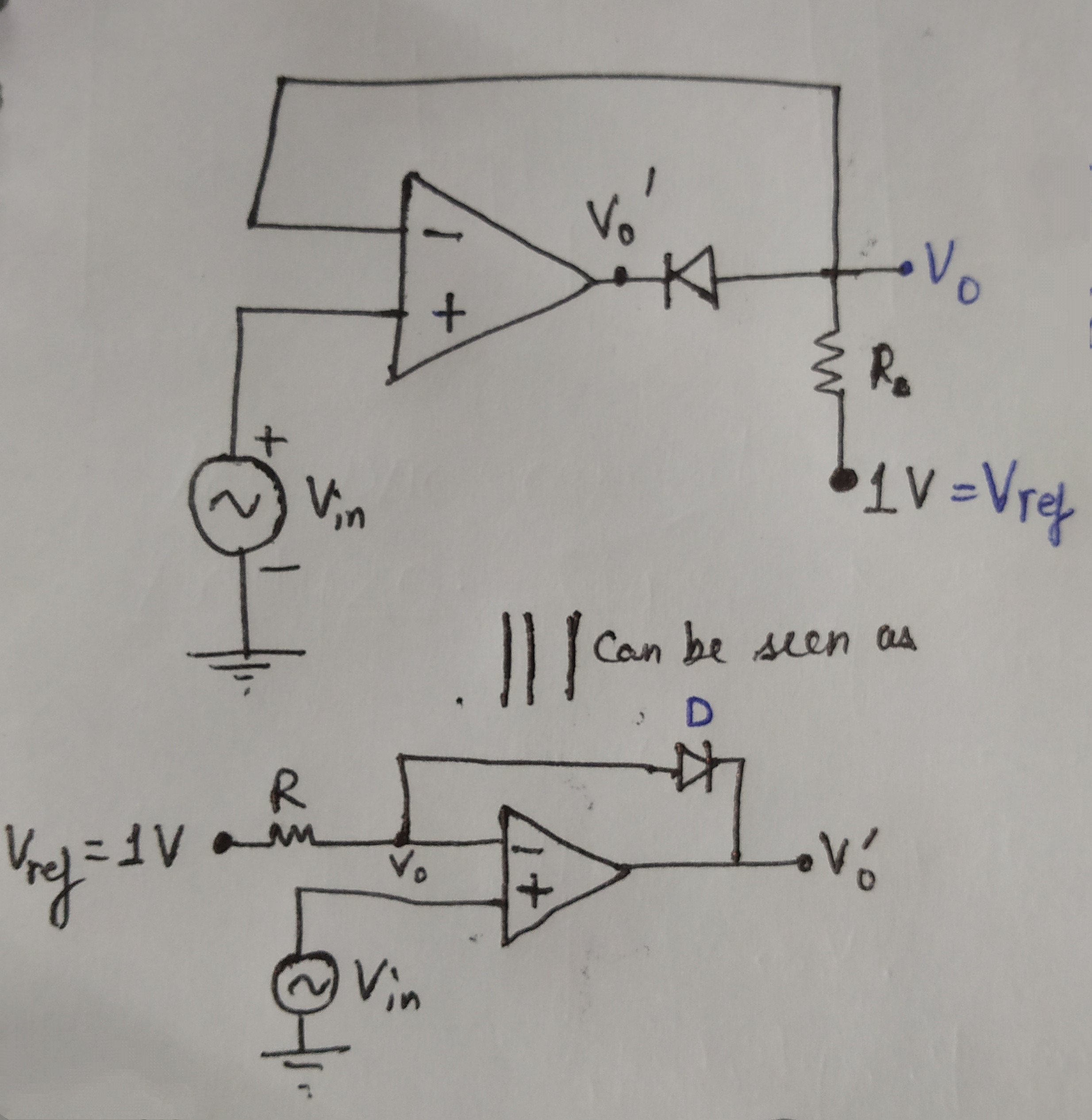
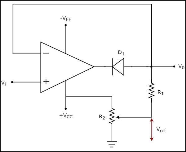
This specific circuit solution has long been explained... and probably many more after that. But for all of them to be truly understood, we need to see the general idea behind them.
Let's play around with the circuit in CircuitLab and learn some wisdom about this kind of op-amp circuits with "dynamic negative feedback".
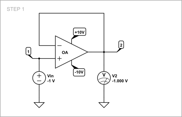
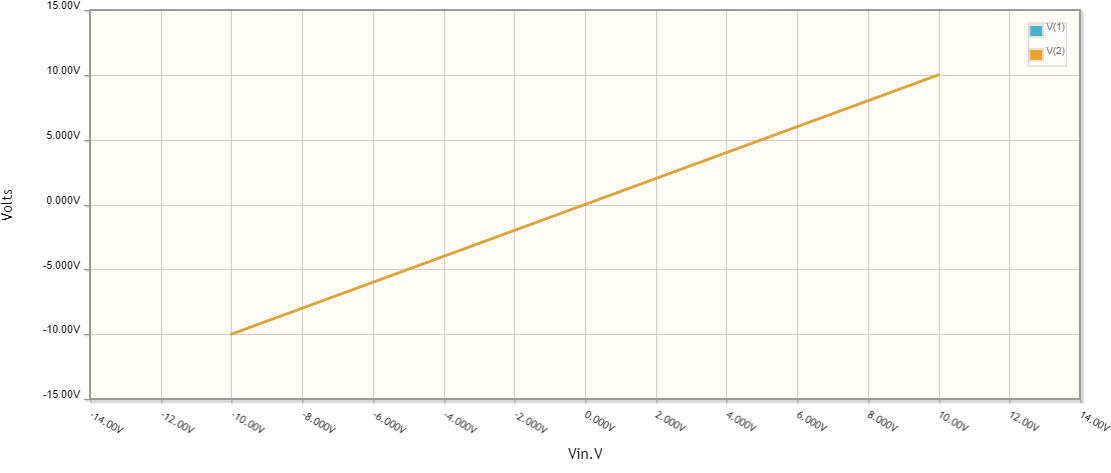
STEP 1: Op-amp follower undisturbed
In a voltage follower, the op-amp effortlessly accomplishes its task of keeping its output voltage equal to the input voltage.

simulate this circuit – Schematic created using CircuitLab

STEP 2: Op-amp follower disturbed
But its task becomes more complicated if some disturbance occurs between its output and the load. Now it has to make an extra effort to overcome it.
Resistance disturbance
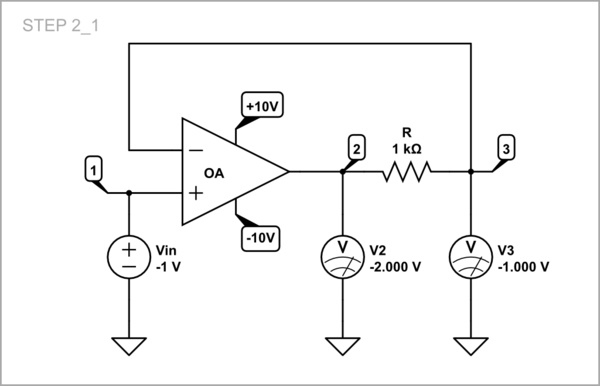
Resistance is the simplest and most common disturbance to an op-amp. Then let's put a 1 k resistor in the op-amp output to see how it will react to our intervention. Let's also connect two voltmeters - before (V2) and after (V3) the resistor.
To simplify the circuit, let's apply a little trick that CircuitLab allows us to do - instead of connecting a load, make the voltmeter V3 perform its function. To do this, open the V3 parameters window and set a relatively small resistance (1 k), i.e., deliberately "worsen" the voltmeter. So remember that V3 is actually a 1 k resistor (just "voltage-visualized"). With the same success, we can replace R with a 1 k "bad" ammeter, but let's not overdo it :-)

simulate this circuit
We see that with a -1 V input voltage applied, the op-amp is forced to produce twice the output voltage (-2 V) in order to have a -1 V voltage across the "load" (V3). Thus of that 2 V, 1 V is lost across the resistor, and 1 V is left for the load.
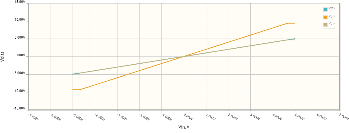
From the DC sweep simulation below, we see that the op-amp is actually forced to amplify 2x before the disturbance to follow 1x it.

This is actually the idea of a non-inverting amplifier that we arrived at in a natural way (not as in the textbooks given ready-made). Let's state it and put it in the "bag of circuit tricks": A non-inverting amplifier is a "deliberately disturbed" follower.
Voltage disturbance
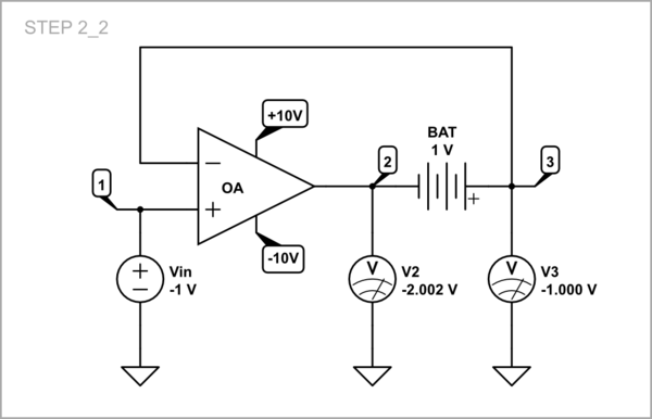
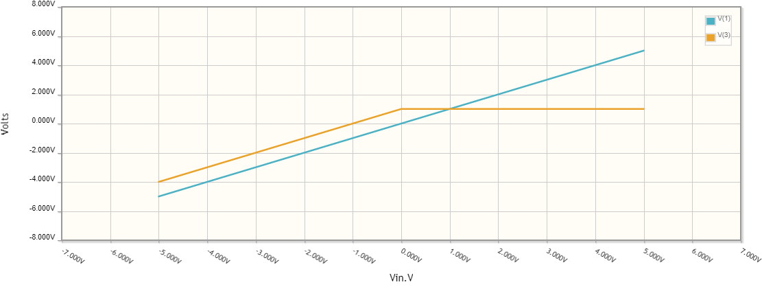
Now we can "provoke" the op-amp with various disturbances to see how "reliable" it is. Thus, the resistance above was linear (proportional, multiplicative) disturbance. Let's now try with some nonlinear (constant, aditive) disturbance, for example with a constant voltage source. It is "floating"; so let's use a battery with the same voltage (1 V) as the voltage drop across R above (I have chosen illustrative convenient values of the quantities).

simulate this circuit
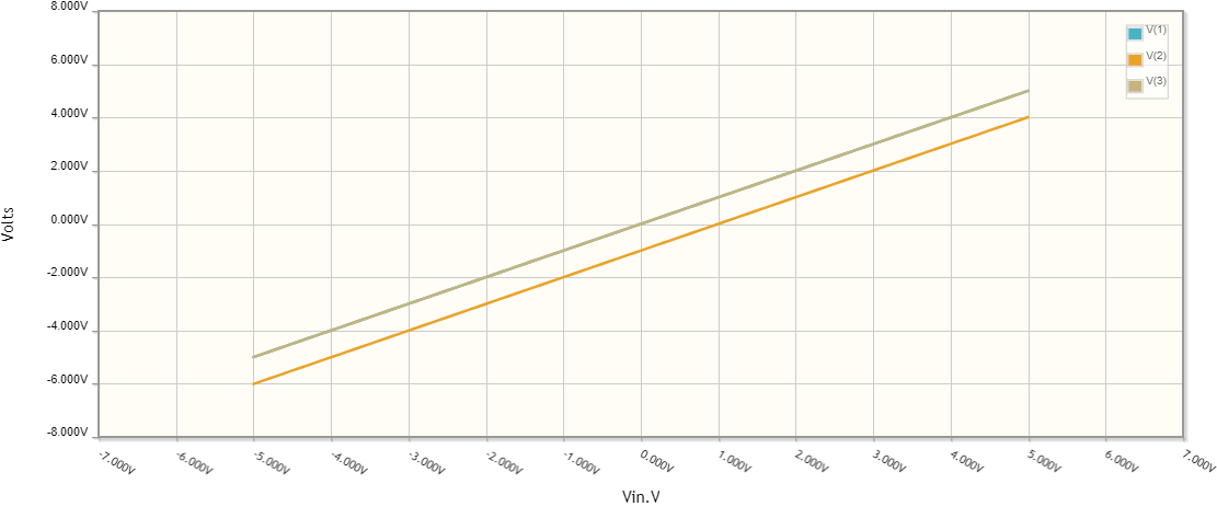
Now, the op-amp steps down its output voltage by an additional constant value of 1 V to compensate for this constant voltage disturbance.

Low diode disturbance
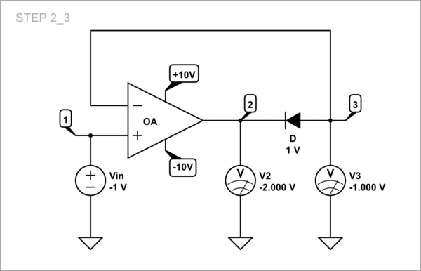
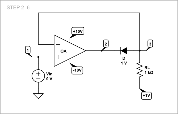
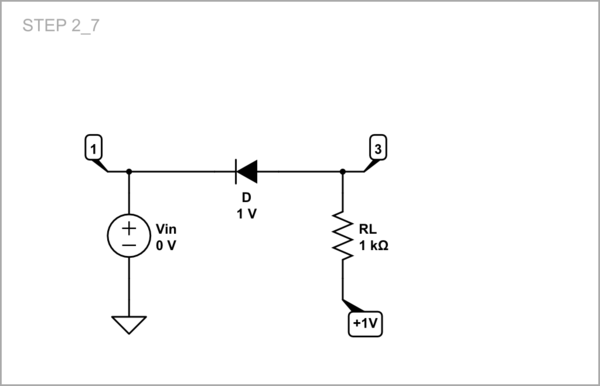
Diodes, like batteries, maintain a constant voltage across themselves when forward-biased. Then let's replace the battery with a diode and thus get even closer to the OP's circuit. For simplicity, I have used an "ideal" diode from the CircuitLab library and ajusted its forward voltage to the favorite 1 V.

simulate this circuit
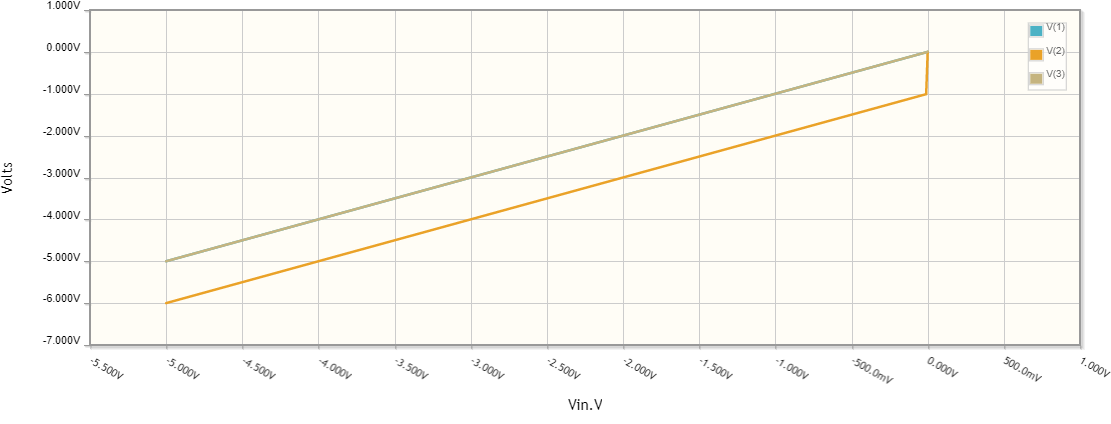
So, when the input voltage is negative, everything is the same as above because the diode behaves as a "battery".

High diode disturbance
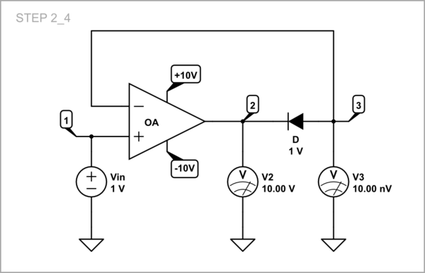
But at a positive input voltage, the diode is reverse biased and the op-amp's task becomes overwhelming.

simulate this circuit
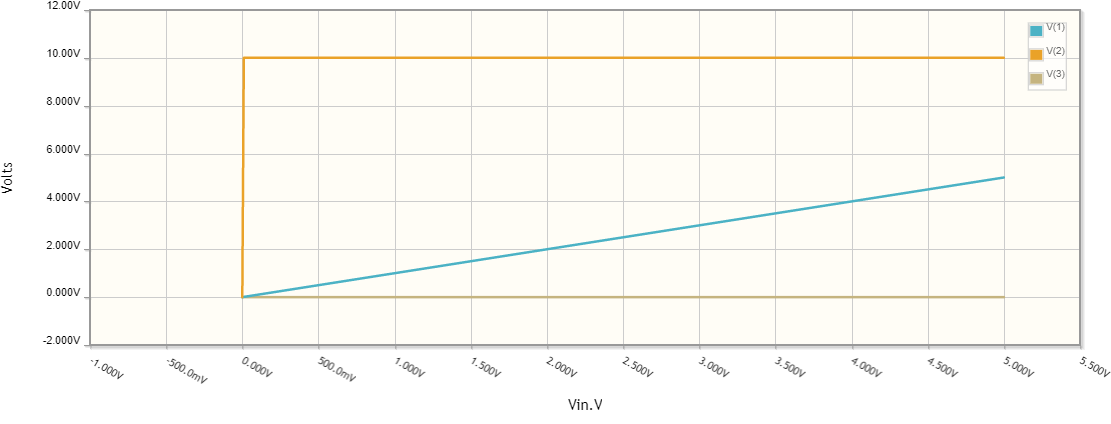
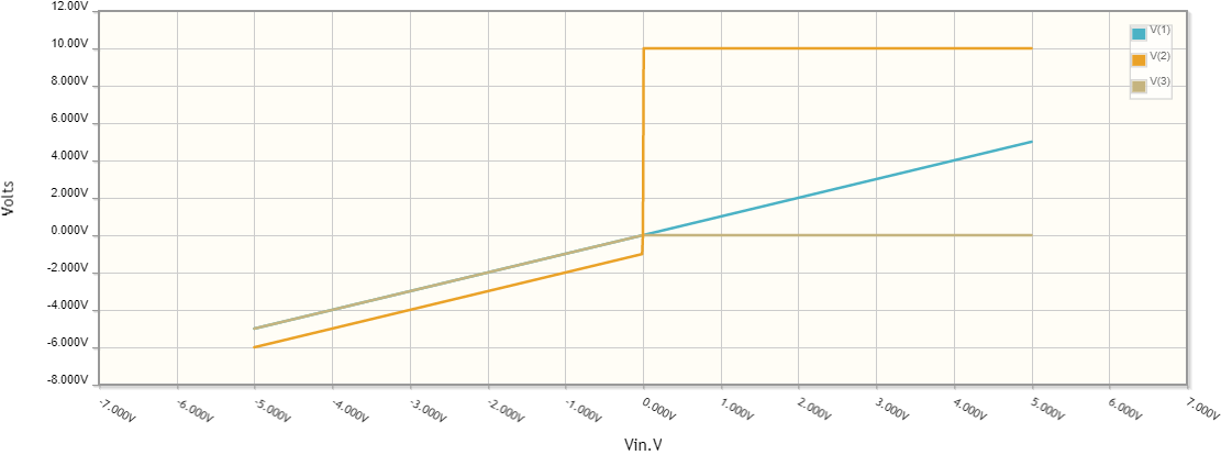
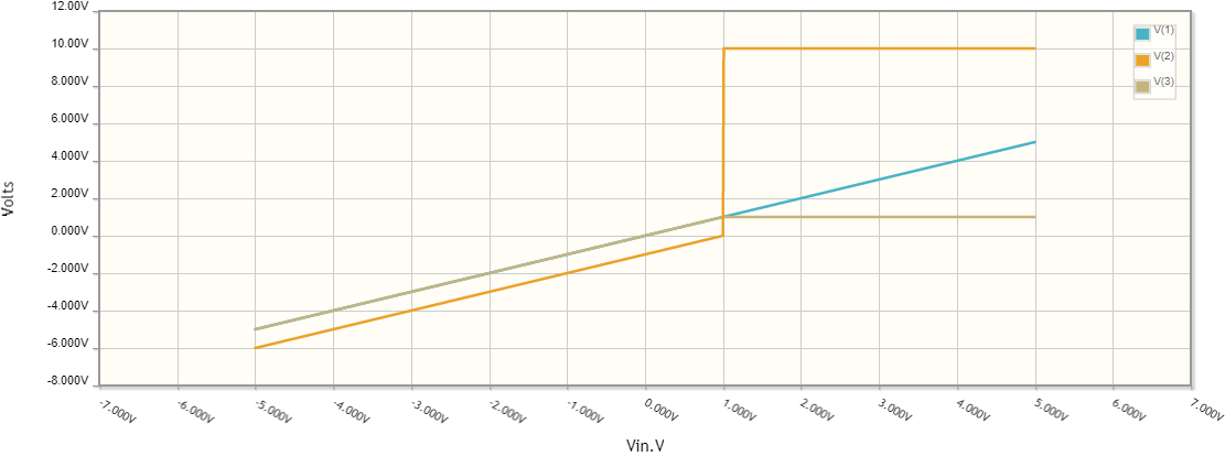
In an effort to compensate for this gigantic disturbance, it continuously raises its output voltage until it reaches the supply voltage and stops there. The output voltage at point 3 is zero since the load connects it to ground.

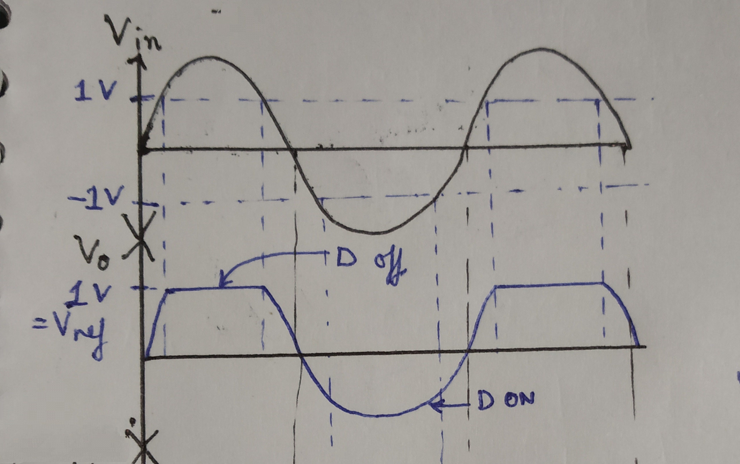
Let's see it over the entire input voltage range (-5 V ÷ 5 V).

So the circuit behaves as a precision zero voltage clipper.
Current disturbance
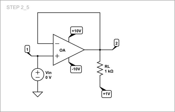
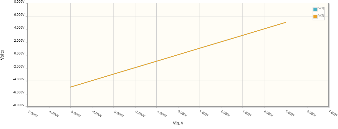
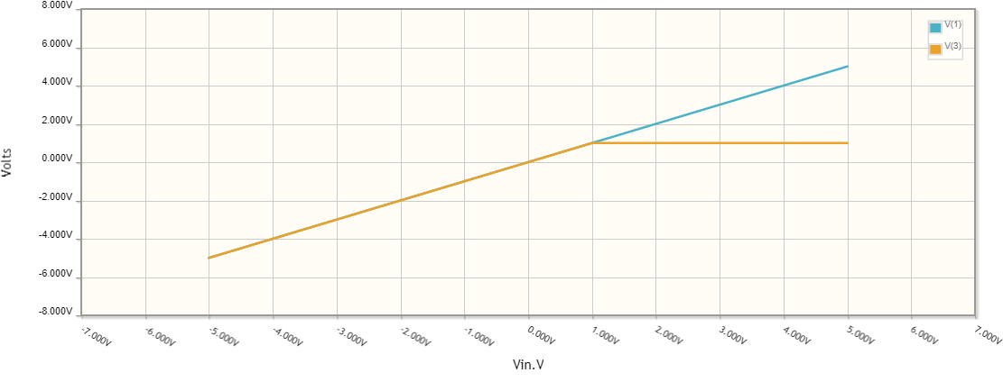
Thanks to these experiments, we gradually realized that an op-amp with negative feedback behaves like an almost "ideal" voltage source because connecting a grounded load does not change its output voltage. And how will it react if we connect the load to some voltage, for example 1 V, instead of ground?

simulate this circuit
It turns out that the op-amp does not care about this and its output voltage exactly follows the input voltage.

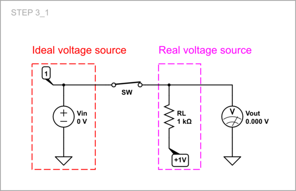
Aha... we gradually start to figure out what is going on here: When connected in parallel with a real voltage source (with Ri = 1 k), the "ideal" voltage source (with Ri = 0) imposes its voltage (0 V) as stronger; when the ideal source us disconnected, the weak real voltage source sets the output voltage at point 3 through the resistance R equal to its voltage (1 V).
Op-amp clipper
So that was the idea behind this op-amp clipper:
If Vin < Vref, the diode switch connects the op-amp output ("ideal voltage source") to the load (real voltage source) and imposes its voltage to the output 3).
If Vin > Vref, the diode switch disconnects the op-amp output from the load supplied by Vref and the latter determines the output voltage (3).

simulate this circuit

Passive diode clipper
The same idea is exploited by the passive version of this clipper circuit only there the diode forward voltage is not compensated and must be taken into account. Also the current of the reference voltage source flows through the input source.

simulate this circuit

If you set VF = 0 V in the D parameters window, the graph will be the same as in the op-amp version above (that is, the op-amp makes the real diode ideal).

STEP 3: The general idea
Finally, let's summarize the idea:
- If we connect an ideal voltage source to a real one in parallel, the ideal source determines the voltage across them.

simulate this circuit
- If we disconnect the ideal voltage source from the real one, the real source determines the voltage.

simulate this circuit
In this way, two voltage sources can be switched to a common load with a simple "on-off" transistor (SPST) switch. In the straightforward solution, they are switched by the more complex SPDT switch.
Of course, this convenience comes at a cost - a higher output resistance in one state. An analogy can be made between these two configurations and the two types of transistor amplifier stages - with a collector resistor and "push-pull".
STEP 4: Implementation
The problem is that we usually only have ideal (perfect) sources. Then we have to artificially worsen an ideal source to make it real (imperfect).
For this purpose, we connect a resistor in series to an ideal voltage source. Thus the combination of the two elements acts as a real voltage source.
STEP 5: What is the resistor for?
It's time to answer the OP's question (a little late indeed, after more than three years :-)
I could not very clearly understand what is the purpose of resistance, R here.
The resistor is needed to "worsen" the reference voltage source. Without it, a conflict between the two ideal voltage sources would result.
