I read since a long time but never had an account, now its my turn to ask a question on here:
I have an idea but currently unsure if that works technically or if it is good design:
1st (Top Layer) : SMD Devices + Routing
2nd Layer : Ground Plane (only Ground)
3rd Layer : Thermal Plane
4rd Layer : Thermal Plane + THD Connections.
So all of my devices are SMD, apart of a few connectors which are THD.
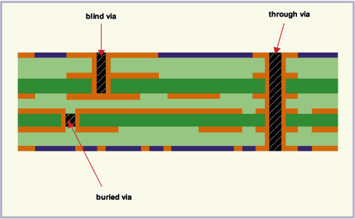
The 3rd and 4rd Layer are only copper planes which are connected to a heat/cold source to regulate temperature of whole PCB. Obviously I will need vias which go only from 1st Layer to 2nd (to ground). Is that maybe too expensive to manufacture?
I am only concerning about my connectors: the pins are soldered on the bottom. Normally THD are like vias, so it also has a connection on the top layer. Which I can connect then to a local ground plane which goes with vias down to the 2nd Layer.
Is that alright?
Maximum Frequency will be about 90 MHz.

