1
\$\begingroup\$

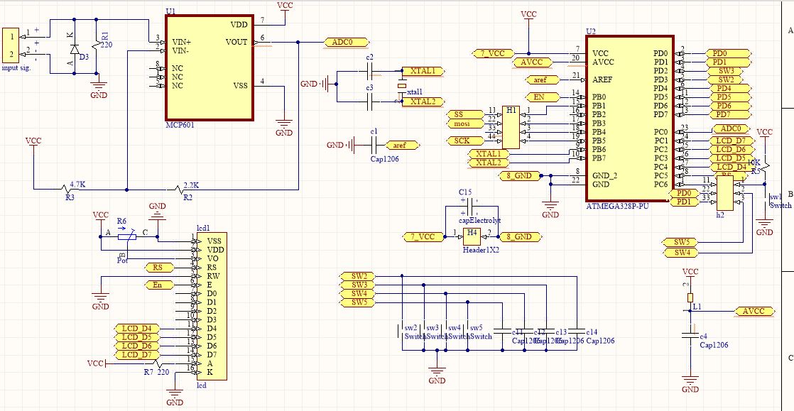
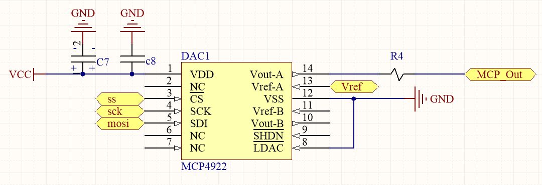
I have designed a 4-20 mA PID controller using an ATmega328P, an MCP4922 (DAC), and an XTR115UA (4-20 mA current loop transmitter).

I used the circuits proposed in the datasheets and the PCB and schematic files are linked.

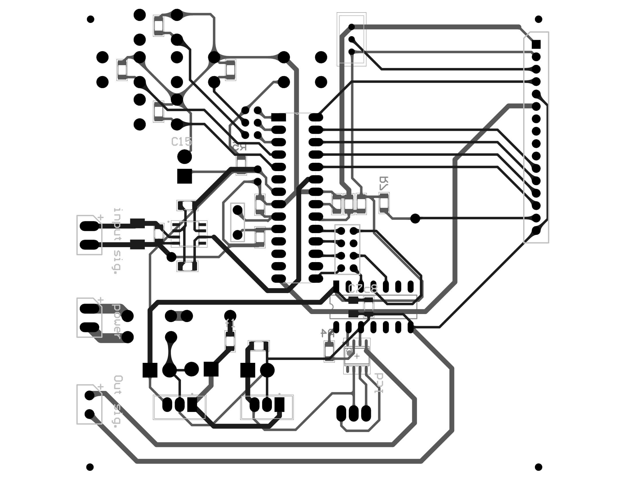
Please have a look and give feedback on the layout or schematics; will this work or fail?

Is it helpful to use a polygon pour on both the top and bottom layers and connect one layer to Vcc and another to GND?

Here are the schematics and PCB.

This is where the 4-20 mA input signal comes in and is converted to a 0-5 V voltage with an MCP601 op-amp. The result goes to the uC:

enter image description here

5 V supply:

enter image description here

The uC output is sent to the DAC:

enter image description here

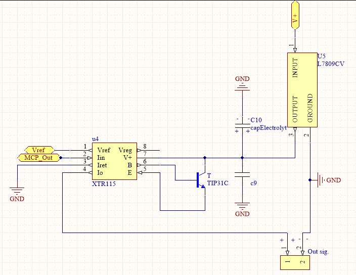
The DAC drives the XTR115 current loop transmitter:

enter image description here

The 7809 produces Vloop and the 4-20 mA output signal goes to an 180 Ω coil.

This is the layout:

enter image description here

\$\endgroup\$
4
  • \$\begingroup\$ Please include the schematic in the question so it will still make sense when the link dies. \$\endgroup\$
    – Transistor
    Commented May 26, 2020 at 7:14
  • 3
    \$\begingroup\$ Nobody with any sense is going to download those files. \$\endgroup\$
    – Andy aka
    Commented May 26, 2020 at 9:44
  • 3
    \$\begingroup\$ Why are some of the ground symbols pointing to the sky? \$\endgroup\$
    – Transistor
    Commented Jun 2, 2020 at 21:20
  • \$\begingroup\$ Worth being specific about R1 in terms of tolerance, etc: specifying a temperature-stable, precise resistor. This is entirely responsible for converting 4-20mA to 5V. Even with calibration, if you have a resistor with a poor temperature stability your circuit will go out of calibration with tempe change. Also, you could be disipating up to 100mW into it, and thermal resistance is of the order of 200K/W, so you can expect about 0.1% temp drift from a typical resistor ~20ppm/K, but this is stuff you need to calculate for your specified resistor and mounting if you want sensible values. \$\endgroup\$
    – Dan
    Commented May 18, 2023 at 8:14

1 Answer 1

1
\$\begingroup\$

Two things that you should consider fixing:

  1. your loop should not be interrupted by LM780x as you want the current to be driven by T1 only. So LM780x input should be in parallel of T1 and then feeding the rest of the board.
  2. if you want the current output to be compensated for variations of your uC is to have the GND node connected to iRet as the datasheet mentions and not

IRET: All return current from IREG and IREF

XTR115 datasheet - FIGURE 1.

Otherwise A1 in the block diagram cannot compensate for variations across R2 which will be coming from U3 and DAC1 in your schematics.

\$\endgroup\$
1
  • \$\begingroup\$ it seems some port names got hidden after converting the schematics to image and now new corrected schematic images was replaced. thank you @AuberonVacher for your help but I can't understand you(maybe for my poor english). "V+" port is the 12 volt input voltage that goes to 7809 input and creates the 9 volt Vloop(and this voltage is fed to pin #7 of xtr115 which accidentally has the same name V+) and as mentioned in XTR115 datasheet this Vloop voltage has to be in series by RL. Do you mean that in my loop schematic, RL and Vloop are not connected in series? – \$\endgroup\$ Commented Jun 9, 2020 at 3:33

Your Answer

By clicking “Post Your Answer”, you agree to our terms of service and acknowledge you have read our privacy policy.

Not the answer you're looking for? Browse other questions tagged or ask your own question.