1
\$\begingroup\$

I want to generate square wave but there are some challenges. Rise time should be less than 2ns as well as fall time (for 0V to 5V). Duty cycle is not so important it should stay high like 40 ns. I am searching for a solution I found these ones but I am not sure if they work for that much high frequency:

  1. Using an FPGA

  2. rf2506 signal generator

  3. ADCMP580 Voltage Comparator. (in data sheet it says 37 ps typical output rise/fall)

  4. Using basic inverting schmitt trigger circuit.

  5. Using high frequency crystal oscillator with schmitt trigger.

Does anyone have an idea about these ideas? Or should I try different method?

\$\endgroup\$
3
  • 6
    \$\begingroup\$ Your timing values don't make any sense. The period of a 500 MHz signal is just 2 ns. \$\endgroup\$
    – Dave Tweed
    Commented Sep 13, 2020 at 16:38
  • 7
    \$\begingroup\$ "should stay high like 40 ns" and "500MHz" are mutually incompatible. (plus a 3ns rise time is already 1.5x the period) You'll need to clarify what you really want beyore worrying about how to do it. \$\endgroup\$
    – user16324
    Commented Sep 13, 2020 at 16:38
  • \$\begingroup\$ Actually you are right I was only considering about rise and fall times. So I didn't look at the real frequency. I am going to edit the question as soon as posible. \$\endgroup\$
    – Ismail
    Commented Sep 13, 2020 at 17:51

5 Answers 5

2
\$\begingroup\$

I've built like three pieces of a simple pulse generator, with 5V supply, that throws a pulse of 30-40 ns long, active high, every 1 ms or so.

reflectometric probe / pulse generator

Click for a PDF version.

I'm using it as a TDR probe for my digital oscilloscope. It works pretty well. I guess the 74AC/ACT logic might just about work for your purposes. Or you can try 74ABT, that's even faster, but IME only reaches about 4V when in log.1.

This is at 50 ns per div, with 74AC04 as a line driver:
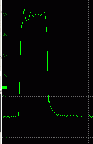
pulse shape

I actually have a web page, showing the early padboard version of this toy. By now I have a proper PCB, and I already know that I should've left a hole in the GND copper fill under the terminator array (its parasitic capacitance to GND acts as a low impedance at the highest frequencies, which impairs the impedance match to the transmission line).

Regarding the question about ripple: given that I'm using this as a simple reflectometer, I do not care much about it. Yes I do wonder where that ripple comes from. It might be the switch (FET) at the output of the gate overshooting a little - for the ugly detailed reasons why FET's sometimes can be observed doing this :-) It might be the output interacting with the complex load impedance. And power supply blocking. Or the ripple may come from the fact that I'm using several gates connected parallel for a higher drive capability (when testing lines down to 50 Ohms nominal) = each gate "fires" at a slightly different moment.

This is approximately what my PCB looks like:
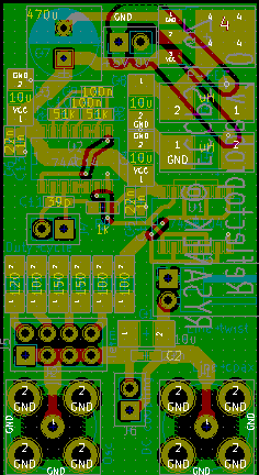
PCB zoomed out

The dimensions are about 30 x 55 mm. Click here if you're interested in the complete KiCad project.

As for power blocking, I have 22n parallel with 1n, as close to the Vcc input of each chip (package) as possible.

Also, note that the pulse shape screenshot is taken by an oscilloscope. There are no probes in play, the probe plugs straight into the scope's input BNC jack. I.e. no probe cables to blame, in this case :-) otherwise they'd be another potential source of "ringing" (probe cable acting as a quarter wavelength TML section for instance). Actually the v1.0 on a proper PCB has a slightly longer connection to the scope (using a BNC M-M coupling) compared to my original padboard prototype, where I bolted a panelmount male to the padboard using a snippet of shaped steel sheet (not chewing gum and duct tape, but almost).

I don't have a screenshot around this time, but I can tell you that the circuit on a proper PCB with a fast 74ABT04 exhibits an even wilder ripple. As a possible partial cause, I suspect the nice large ground plane, occupying most of the solder side of the double-layer PCB. Specifically the output section, featuring relatively broad traces and the pack of resistor (jumper-selectable terminators) probably has non-trivial capacitance against GND, thus slowing down the pulse edges a little, but also making the output harder to the transmission line, than it should be. The "forking" of the signal towards the scope and towards the measured line has a similar effect (the stub toward the scope should be as short as possible). I can see this excess capacitance on scope traces where the far-end reflected pulse gets re-reflected from the signal source (pulse generator) - where I get just short glitches reflected, as the impedance matching is not exactly right at high frequencies. (I'll add an example trace if I get one.)

So my general advice, if you're concerned about the ripple:

  • make the PCB layout as small as possible. Parasitic inductances and capacitances all boil down to physical dimensions of the signal paths. Larger dimensions make any parasitic self-resonant frequencies move down, where the silicon also has more gain, resulting in more potential for glitching and ringing.
  • pay attention to power blocking for the chips
  • pay attention to impedance matching, from signal source to signal sink, and also how your oscilloscope input is attached = tapped/coupled into the circuit under test). My circuit is fairly universal = contains too many parts and extra traces specifically in the output signal path, that hardly ever get used, just add parasitic capacitance. You can probably skip some of the bloat, by reducing the circuit to a bare minimum necessary for your "application".
  • be aware of the limits of your oscilloscope and probes.
  • if you need to use connectors, consider using something smaller: SMA, MCX, MMCX, U.FL or some such. Those BNC's are humongous beasts.
\$\endgroup\$
3
  • \$\begingroup\$ Thanks a lot. I think it might work for me. I will try it as soon as possible. But only problem here I think is ripple. Do you know a way to suppress it. Should I clamp with zeners at output? Or some decoupling capacitors will work? \$\endgroup\$
    – Ismail
    Commented Sep 27, 2020 at 21:22
  • \$\begingroup\$ @Ismail I have added a couple paragraphs to my answer to address your comment. \$\endgroup\$
    – frr
    Commented Sep 27, 2020 at 22:35
  • \$\begingroup\$ case of need of faster rise time ... something as sn74lvc1g132 is usefull. or sn74auc00.pdf \$\endgroup\$
    – Antonio51
    Commented Sep 28, 2021 at 19:24
3
\$\begingroup\$

500-600 MHz will need rise/fall times in the sub-1ns range. You will need to consider advanced driver techniques like differential HSTL, LVDS, HSCL, etc to achieve this. These kind of clock rates are what you find on DDR3.

TI and others make a range of clock generators that can do this. An FPGA that’s DDR3-capable can do it.

\$\endgroup\$
2
  • \$\begingroup\$ I am sorry for late reply. Sorry in my question I didn't state voltage range. I edited my question. I need 0V-5V range. So HSTL, LVDS etc are not for my application. Do you think FPGA can generate 0V - 5V with 2 or less nanosecond rise time? \$\endgroup\$
    – Ismail
    Commented Sep 27, 2020 at 21:05
  • \$\begingroup\$ Not directly. You will need to choose a suitable buffer / level shifter. \$\endgroup\$ Commented Sep 28, 2020 at 15:14
1
\$\begingroup\$

If the 40ns period time is also good, the choice is increased. Here is one right now that knows more than that. (Output Rise/Fall Time (10% - 90%)V+ = 5.5V, RLOAD = ∞, CLOAD = 5pF 1ns.)

\$\endgroup\$
2
  • \$\begingroup\$ Yes, it might also work. But isn't the driver improtant when I try to reach 1ns rise time. I mean if pic (in the typical test circyit) trigger slow, then also ltc will rise slow and won't reach 1ns. Am I correct? \$\endgroup\$
    – Ismail
    Commented Sep 28, 2020 at 4:53
  • 1
    \$\begingroup\$ The shape of the output signal is independent of the control. One problem, however, will be the load on the output signal. "It is strongly suggested that a high speed buffer is usedwhen driving more than one or two logic inputs, whendriving a line more than 5 centimeters in length, or acapacitive load greater than 5pF." \$\endgroup\$
    – csabahu
    Commented Sep 28, 2020 at 7:49
0
\$\begingroup\$

Use a commercial ECL oscillator . It can operate up to 1100MHz. Its output is an ECL level rectangle with 0.77V amplitude.

555 MHz oscillator: 555mhz

\$\endgroup\$
3
  • \$\begingroup\$ Sorry for late response I edited the question. It should be 0V to 5V level \$\endgroup\$
    – Ismail
    Commented Sep 27, 2020 at 20:15
  • 1
    \$\begingroup\$ I see a fundamental change in the situation, no longer need 500 MHz, but only 25MHz? (40ns?) \$\endgroup\$
    – csabahu
    Commented Sep 27, 2020 at 22:46
  • 1
    \$\begingroup\$ You also need to specify your load. Is it 50 ohms? A coax cable? If a cable, how long? if a pcb trace, what impedance and how long? Keep in mind that , for instance, 5 volts into 50 ohms is going to require 100 mA. And driving a 100 pF cap to 5 volts in 1 nsec will require an average current of 500 mA. \$\endgroup\$ Commented Sep 28, 2020 at 1:35
0
\$\begingroup\$

You can use programmable PLL clock synthesizer, like NBC12439AMNG with up to 800MHz PECL output.

\$\endgroup\$

Your Answer

By clicking “Post Your Answer”, you agree to our terms of service and acknowledge you have read our privacy policy.

Not the answer you're looking for? Browse other questions tagged or ask your own question.