0
\$\begingroup\$

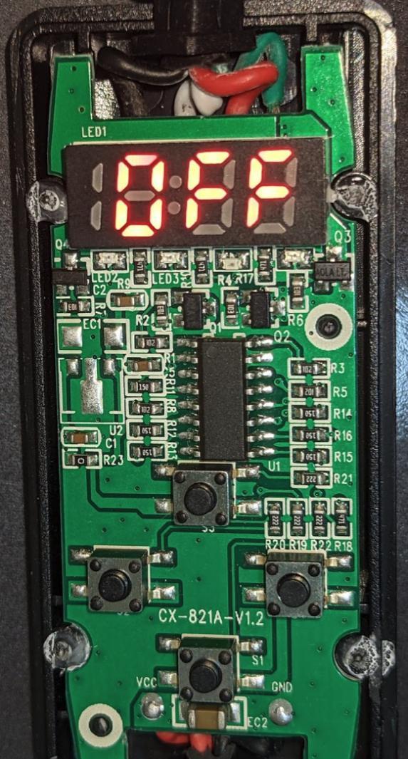
I was hoping someone could help me decipher this Q4 PNP transistor. It is labeled Y2 on top of it but it didn't come out in the image. Looking around on google I see that it is a PNP transistor and looks like it is probably very similar to this one here.

All of the components I am worried about are pictured on the top of the PCB.

There are some strange things going on there that I am uncertain about inbetween the transistor's base and emitter, and the R7 10k (103) resistor that I am hoping a more experienced eye will be able to figure out.

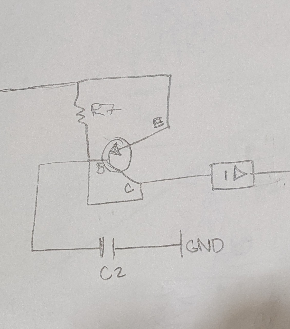
Does my interpretation look sane?
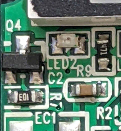
PNP Transistor labeled Y2

Attempt and circuit schematic here:
Attempt at sub-circuit schematic

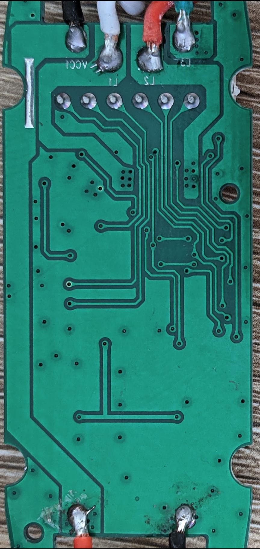
Mirrored Back of pcb

enter image description here

\$\endgroup\$
6
  • 1
    \$\begingroup\$ There's probably a via under the transistor where you are showing a connection to the collector. \$\endgroup\$ Commented Jan 10, 2021 at 22:08
  • \$\begingroup\$ @SpehroPefhany It doesn't look like it. I added the image of the back mirrored as if you could look through the board. \$\endgroup\$
    – Bob R
    Commented Jan 10, 2021 at 23:04
  • \$\begingroup\$ Hi BobR. Getting things correct is really a requirement but it seems has you have started off in the wrong direction from the outset. In your text you go on about a Q1 whilst your PCB picture does not even show a Q1. Let's see if this can be straightened out before proceeding forward. \$\endgroup\$ Commented Jan 10, 2021 at 23:23
  • \$\begingroup\$ @MichaelKaras yep your right, that is supposed to be a Q4 there. Fixed. \$\endgroup\$
    – Bob R
    Commented Jan 10, 2021 at 23:30
  • \$\begingroup\$ The chances are that the tracks under the transistor don't go where you think they do. \$\endgroup\$
    – Simon B
    Commented Jan 11, 2021 at 0:01

0

Your Answer

By clicking “Post Your Answer”, you agree to our terms of service and acknowledge you have read our privacy policy.

Browse other questions tagged or ask your own question.