0
\$\begingroup\$

So this is part of a theoretical design problem that I've come across not too long ago, and still can't find a satisfactory answer for it.

Assume a large (infinite) metal plane with a round hole in it of size \$d\$.

Further assume an RF transmitter one side of the hole, and a receiver on the other, some distance away from that hole. In case the diameter is zero (no hole) the attenuation of the screen is 100%, and if the screen is gone, the attenuation is only dependent on the distance between the transmitter and the receiver (I'm assuming omnidirectional transmitter elements and receivers here).

Now, to my understanding, how much of the RF energy is passed through the hole is dependent on how large the hole is in relation to the wavelength. In my mind, the hole will act like a screen, but it will also cause the wave pattern to refract. However, as I understand it, the hole needs to be at least \$\dfrac{\lambda}{2}\$ in diameter, otherwise the attenuation will be extremely high. Am I right in this assumption? And what is the general correlation with screens like this, for instance, depending on the polarity, a square hole might let some RF through in one orientation and not in the other, but what about CW and CCW polarized RF?

I'm perfectly happy with a bunch of pointers to resource material I can read myself up on.

Thanks!

\$\endgroup\$
4
  • \$\begingroup\$ Fields can diffract through small holes, analogous to how a (deeply subwavelength) molecule of gas in the atmosphere can defect a (very small) amount of a plane wave via Rayleigh scattering. Once you get below a wavelength, the amount of field coupling through drops rapidly, but it doesn't go to zero as long as the hole is there. Usually though there is some minimum amount of field you can tolerate (e.g. pass EMC) and going lower doesn't matter. \$\endgroup\$ Commented May 13, 2021 at 13:55
  • \$\begingroup\$ Also note that it doesn't have to be hole. A thin slot with a length the same as the hole diameter can allow just as much RF through as the hole. This is the reason EMI gaskets are used on chassis covers. \$\endgroup\$
    – SteveSh
    Commented May 13, 2021 at 14:06
  • \$\begingroup\$ You will find some answers if you search long enough on Google. You might need to use the term Evanescent Wave. There are (empirical) formulas for leakage through holes much smaller than lambda, one hole or many. The thickness of the metal also matters. \$\endgroup\$
    – tomnexus
    Commented May 13, 2021 at 15:33
  • \$\begingroup\$ @user1850479 I'm aware, I said circular hole, so that polarisation isn't an issue. But I'm still wondering how circular polarized RF works with ports in a screen like that. \$\endgroup\$
    – polemon
    Commented May 13, 2021 at 15:48

2 Answers 2

5
\$\begingroup\$

The hole size needs to be << 10 % 𝜆 for high impedance mismatch and high return loss. The transmission loss near 𝜆/2 and all multiples will be minimum and the leakage might be computed by a function of the ratio of shielded to aperture ratio at those minimum loss wavelengths. I cannot offer a quick formula, however.

Anecdotal

I recall buying the surplus Stanley Door company 120 dB Lindgren Faraday cage from KJ Marketing in Toronto 25 yrs ago and we constructed the double walled copper “bug screen” and beryllium copper fingered doors on the double clamped frame corners in a day in the lab in Winnipeg. It was the size of a large gazebo. It wasn’t exactly -120 dB over the whole range up to 20GHz but perfectly adequate to perform telemetry isolation tests and adjacent channel interference tests free from ambient noise. I designed an optimal integrate and dump RSSI board and the H/W guys built it same day while data collection was automated for graphical results at the same time. This was a design validation test for how many million transmitters can you squeeze in a narrow channel with the smallest guard bands,by measuring the SNR of an optimal receiver (I&D) for both the signal and RSSI level both using integrate and dump detection for the purpose of automated power meter telemetry reading licensed channels owned by power utility companies near 928MHz using TDM, FDM, spacial colouring with pleisiochronous signalling for the AMR business that outperformed any spread spectrum 2 way trial.

\$\endgroup\$
5
  • 4
    \$\begingroup\$ The Ott book agrees… there's a whole section on it (6.10 apertures, from page 267). A single hole is 'computed' as a slot antenna, and there are formulas. Multiple aperture are more empirical (2D arrays are 'reduced' to 1D, it's quite a mess). In general is way better to use a lot of small holes than a bigger single one (look at the honeycomb pattern in PC power supplies, that's the principle in action) \$\endgroup\$ Commented May 13, 2021 at 14:43
  • \$\begingroup\$ but also note that these 1D approximations are misleading, at times. I remember not that many years (6?) in the past when someone went back and actually simulated a whole lot of textbook Faraday cage examples, and none actually worked well as such, whereas the microwave oven doors work better than simple analytical reductions allow to infer. Truth be told, if you have a 3D problem where boundary conditions are pretty dominant (such as in a small cage with holes), then simulation might your only way out. Reducing 2D to 1D works beautifully when you can actually assume infinite periodicity :( \$\endgroup\$ Commented May 13, 2021 at 15:37
  • \$\begingroup\$ ah, there we go: physicsworld.com/a/… , and the paper that gathered quite a bit of interest in 2015: people.maths.ox.ac.uk/trefethen/faraday_published.pdf \$\endgroup\$ Commented May 13, 2021 at 15:42
  • \$\begingroup\$ OK, that's pretty cool, if you guy could perhaps suggest a book or something, that'd be awesome. Papers are fine, too. \$\endgroup\$
    – polemon
    Commented May 13, 2021 at 15:49
  • \$\begingroup\$ @polemon see my answer. \$\endgroup\$ Commented May 13, 2021 at 16:01
1
\$\begingroup\$

The only way to know is to simulate, honestly.

As Tony explains (I've upvoted his answer), holes need to be small to look like solid conductor. Even then, it's a slot antenna, and can be an emitter for frequencies much lower (wavelengths much larger) than the hole size would suggest.

It's really not sufficient to consider a mesh just an array of holes that "are opaque to larger wavelengths". As numerical analysis shows, the conductor distance plays, at least in a circular 2D scenario, which is the classic thing to "project" down to a 1D problem, less of a role than conductor diameter:
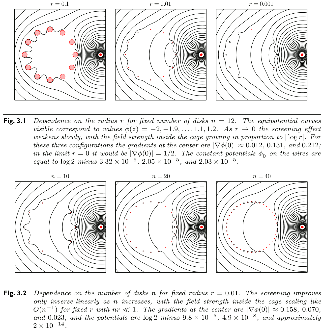
Figures 3.1 and 3.2 from Chapman, Hewett, Trefethen: Mathematics of the Faraday Cage, 2015Figures 3.1 and 3.2 from Chapman, Hewett, Trefethen: Mathematics of the Faraday Cage, 2015

So, there you go, conductor properties play a role that at the very least rivals the importance of the size of holes. Which is counter-intuitive for many of us engineers (including me).

What that means: Unless you know what you're doing whilst simplifying the geometry to come to a conclusion on the effectiveness of shielding, don't do that simplification.

Since simulation isn't hard, do it. If you got access to CST studio, great, then you can import CAD drawings, fully simulate, etc (there's certainly other commercial EM simulation software, too); if you don't, try OpenEMS, which is especially nice if you have easy-to-define geometry like a box with a hole.

Of course, you can also solve things by foot in Matlab or octave, as the authors of the paper cited above did:

% Solve the problem:
n = 12; r = 0.1;
c = exp(2i*pi*(1:n)/n);
rr = r*ones(size(c));
N = max(0,round(4+.5*log10(r)));
npts = 3*N+2;
circ = exp((1:npts)’*2i*pi/npts);
z = [];
for j = 1:n
    z = [z; c(j)+rr(j)*circ];
end
A = [0; -ones(size(z))];
zs = 2;
rhs = [0; -log(abs(z-zs))];
for j = 1:n
    A = [A [1; log(abs(z-c(j)))]];
    for k = 1:N
        zck = (z-c(j)).^(-k);
        A = [A [0;real(zck)] [0;imag(zck)]];
    end
end
X = A\rhs;
e = X(1); X(1) =[];
d = X(1:2*N+1:end); X(1:2*N+1:end) = [];
a = X(1:2:end); b = X(2:2:end);

% Plot the solution:
x = linspace(-1.4,2.2,120);
y = linspace(-1.8,1.8,120);

[xx,yy] = meshgrid(x,y);
zz = xx+1i*yy;
uu = log(abs(zz-zs));
for j = 1:n
    uu = uu+d(j)*log(abs(zz-c(j)));
    for k = 1:N, zck = (zz-c(j)).^(-k); kk = k+(j-1)*N;
        uu = uu+a(kk)*real(zck)+b(kk)*imag(zck); end
    end
    for j = 1:n, uu(abs(zz-c(j))<rr(j)) = NaN; end
    z = exp(pi*1i*(-50:50)’/50);
    for j = 1:n, disk = c(j)+rr(j)*z; fill(real(disk),imag(disk),[1 .7 .7])
    hold on, plot(disk,’-r’), end
contour(xx,yy,uu,-2:.1:1.2), colormap([0 0 0]), axis([-1.4 2.2 -1.8 1.8])
axis square, plot(real(zs),imag(zs),’.r’)

(code reportedly needs < 1s to produce leftmost picture in Fig. 3.1; I fully believe that. I pasted it here just to demonstrate there's no good reason not to simulate.)

\$\endgroup\$

Your Answer

By clicking “Post Your Answer”, you agree to our terms of service and acknowledge you have read our privacy policy.

Not the answer you're looking for? Browse other questions tagged or ask your own question.