2
\$\begingroup\$

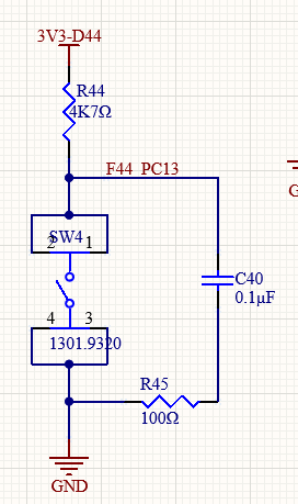
I'm making a prototype PCB with an STM32 chip and I want a couple of tactile switches for various reasons. I have followed the button debouncing circuit as done on the dev board:

enter image description here

My PCB design is physically fairly large (250mm x 150mm) and the buttons are approximately 70mm away from the microcontroller (due to physical constraints). Now my question:

Do I want my resistor and cap (C40 and R45) to be physically close to the button or the microcontroller? Does it even matter?

\$\endgroup\$
3
  • \$\begingroup\$ I'd put it as close as I can, to make it easy to route if nothing else. \$\endgroup\$
    – Hearth
    Commented Jun 17, 2021 at 15:37
  • 1
    \$\begingroup\$ Hi, thanks for the comment but you need to clarify that statement. Is that put caps and resistor closer to the switch or to the MCU? \$\endgroup\$
    – ChrisD91
    Commented Jun 17, 2021 at 15:58
  • 2
    \$\begingroup\$ Put them wherever, 70mm is insignificant in this application. \$\endgroup\$
    – vir
    Commented Jun 17, 2021 at 16:01

3 Answers 3

3
\$\begingroup\$

If you place the cap and resistor close to the MCU, then the trace connecting to the switch will also carry the transient spikes and noise from the bouncing event.

If you place the cap and resistor close to the switch, the bouncing transients will be filtered out, and the trace connecting to the MCU will have a lower dv/dt.

As others have said, given the dimensions in your application, it likely won't matter, but if the trace is routed near something sensitive, noise from switch actuation could couple onto it.

\$\endgroup\$
3
\$\begingroup\$

I will not make any difference to the debouncing. If you suffer from OCD like some of us though put it close to the switch. The bouncing contact may produce EMI.

\$\endgroup\$
2
  • 1
    \$\begingroup\$ Added to the potential EMI: the MCU is generally crowded and switches typically have tons of space around them. \$\endgroup\$
    – Wesley Lee
    Commented Jun 17, 2021 at 16:26
  • \$\begingroup\$ If you have OCD, you would not use that configuration for debouncing to begin with, but look for tact switch manufacturer appnotes for better arrangements. Pushing the button causes 33mA surges and not all tact switches can handle that. \$\endgroup\$
    – Justme
    Commented Jun 17, 2021 at 18:05
-2
\$\begingroup\$

The RC time constant across the switch is 10 us relative to a short bounce time of 1ms for a button or 10 ms for toggle switch indicates R is harmless for the decay time of 0.47 ms but may be slightly low so 10k might be more appropriate to allow increases from mechanical aging.

In gold plated switches if a large e-cap were used to debounce then may reduce the damage of the arc current. So a current limiting Rs seems appropriate. This applies to all metal contact switches up to 2A. It is not known to me if 0.1uF has enough energy to cause pitting in gold plating in 10us, but it’s possible. So IMHO a worthy add-on.

For larger currents >=2A , no switches are gold plated and a large e-cap is desirable to de-wet the oxide insulation on every closure as well as increase the de-bounce time to >=10 ms.

\$\endgroup\$

Your Answer

By clicking “Post Your Answer”, you agree to our terms of service and acknowledge you have read our privacy policy.

Not the answer you're looking for? Browse other questions tagged or ask your own question.