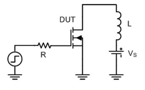
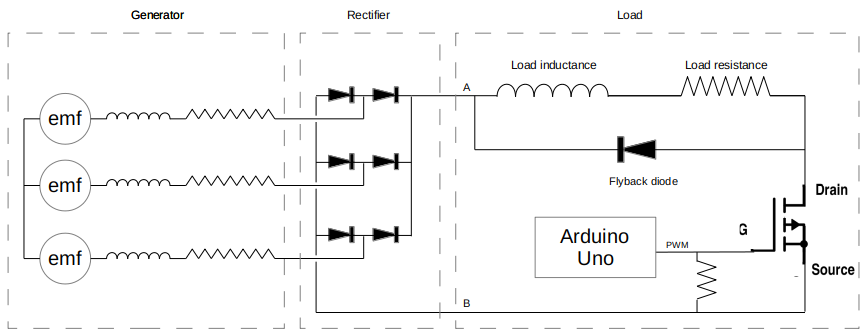
UIS = Unclamped Inductive Spike, some now call it Unclamped Inductive Switching, same thing. This is the transient when power to an inductor is switched off. The inductor reverses polarity the voltage will rise until the energy contained in the inductor is dissipated. An example of that test circuit is shown below. You will find a similar schematic on the MOSFET data sheet with the pertinent details they tested to. We started testing for this in the early 80's for the automotive market. I believe Siliconix was the first to add this to there data sheets. What we saw was UIS devices are basically unlimited in avalanche current until the junction temperature exceeds the intrinsic temperature of approximately 420 degrees C, process dependent, or the bond wires fry. During breakdown we were seeing the device behaving like it was 2X RDSon. Note: secondary breakdown then occurs independent of the parasitic BJT.

From: Ti Understanding MOSFET data sheets, Part 1 - UIS/avalanche ratings.
"The unclamped inductive switching (UIS) rating has proven to be a useful parameter since becoming prevalent in MOSFET data sheets in the mid-1980s. While repetitive avalanching of the FET is not recommended in actual applications, engineers have learned to use this metric to avoid designing-in weaker devices that might cause issues. Devices with particularly weak UIS capability or heavy degradation over temperature (>30 percent from 25°C to 125°C) should raise a red flag, as these devices will be more susceptible to failing. Designers should also be weary of manufacturers playing games with the ratings to exaggerate their FET’s avalanche capability. Not all devices with the same label will support the same amount of UIS, check the data sheet to be sure. Also note during UIS it is heating the junction, to much and it fails.
UIS testing is conducted with a test circuit like the one seen in Figure 1. A supply voltage is applied across the FET while it is turned off and the device is checked for leakage. As the FET is turned on, the inductor current steadily increases. When the desired current is achieved, the FET is switched off and the Ldi/dt voltage across the FET swings above the MOSFET’s breakdown, activating its intrinsic parasitic-bipolar transistor and effectively avalanching the FET. This test is repeated, ramping up the current incrementally, until destruction of the device occurs as evidenced by a failing of the preliminary leakage test."


