0
\$\begingroup\$

I am buiding an OCL amplifier and want to analyze the crossover distortion.

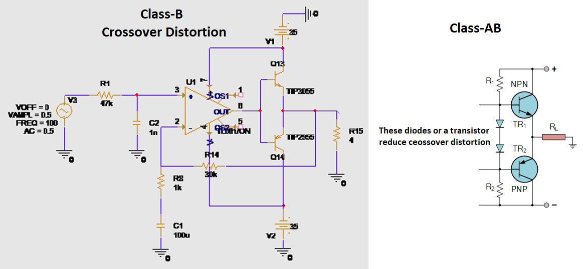
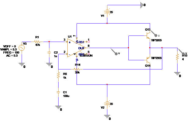
I added 2 power triodes (TIP3055 and TIP2955) as the basic OCL output stage.

enter image description here

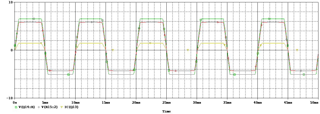
It is weird that there seems to be no crossover distortion on the output waveforms:

enter image description here

Could someone explain why the output waveform is different from the desired crossover distortion waveform?

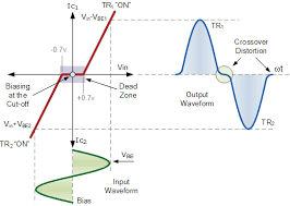
Desired crossover distortion:

enter image description here

\$\endgroup\$
6
  • 1
    \$\begingroup\$ Try a faster signal e.g. some kHz and smaller timestep and see if crossover distortion is visible. \$\endgroup\$ Commented Sep 24, 2021 at 4:37
  • \$\begingroup\$ Thanks lars.It works now. Also, may I know why the output waveform is close to sin wave under high frequency(about 100HZ) but staircase wave under low frequency(100Hz) \$\endgroup\$
    – Linda Yu
    Commented Sep 24, 2021 at 6:57
  • \$\begingroup\$ 2 power triodes???? \$\endgroup\$
    – Andy aka
    Commented Sep 24, 2021 at 8:42
  • \$\begingroup\$ Yes,I got this structure from the book, It's called OCL power amplifier structure. \$\endgroup\$
    – Linda Yu
    Commented Sep 24, 2021 at 9:13
  • 1
    \$\begingroup\$ electronics.stackexchange.com/questions/309936/… \$\endgroup\$
    – G36
    Commented Sep 24, 2021 at 16:45

3 Answers 3

2
\$\begingroup\$

You have a feedback all the way from the output stage (R14). That feedback does compensate for the nonlinearity caused by the Vbe thresholds of the BJT complementary pair. In reality (and looking closely) there will be some amount of distortion as the operational amplifier has a limited slew rate.

If you want to see the distortion in its entire effect in your simulation connect the R14 to the output of the operational amplifier and observe the output.

\$\endgroup\$
0
\$\begingroup\$

Could anyone explain why the output waveform is different from the desired crossever distortion waveform?

Note that in linear applications, cross-over distortion is not desired - it is regarded as a disturbing effect that deviates from desired linearity.

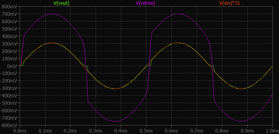
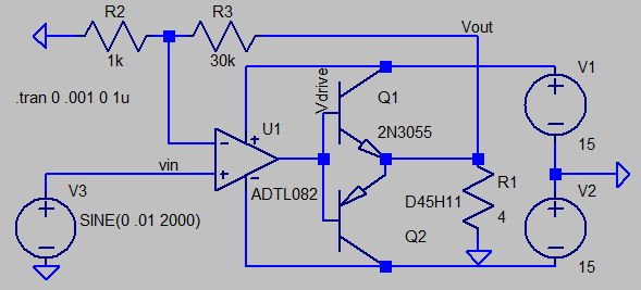
You can see below how the op amp tries to compensate for the cross over effect caused by the two output transistors (see the waveform Vdrive). Op amp gain overcomes much of the cross over problem by slewing its output quickly to provide base current drive so that output waveform Vout follows input waveform Vin.

The op amp is never entirely successful in eliminating the cross over effect, since its slew rate is not infinitely-fast, and its gain is finite. The green waveform (Vout) shows remnants of cross over distortion that the op amp is unable to eliminate. The cross over effect is best seen with a small-amplitude input waveform:amplifier schematic
waveform
There are other problems with your circuit.
Few op amps will withstand \$\pm 35 V\$ power supplies. Furthermore, with a 4-ohm load, many op amps cannot supply enough output current to the bases of the driver transistors for large signal peaks.

\$\endgroup\$
0
\$\begingroup\$

The output transistors in your amplifier operate in class-B but it should be class-AB. Look it up and look here: crossover distortion

\$\endgroup\$

Your Answer

By clicking “Post Your Answer”, you agree to our terms of service and acknowledge you have read our privacy policy.

Not the answer you're looking for? Browse other questions tagged or ask your own question.