1
\$\begingroup\$

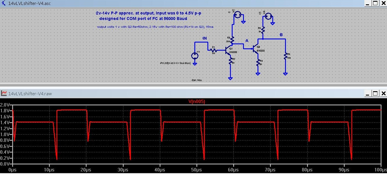
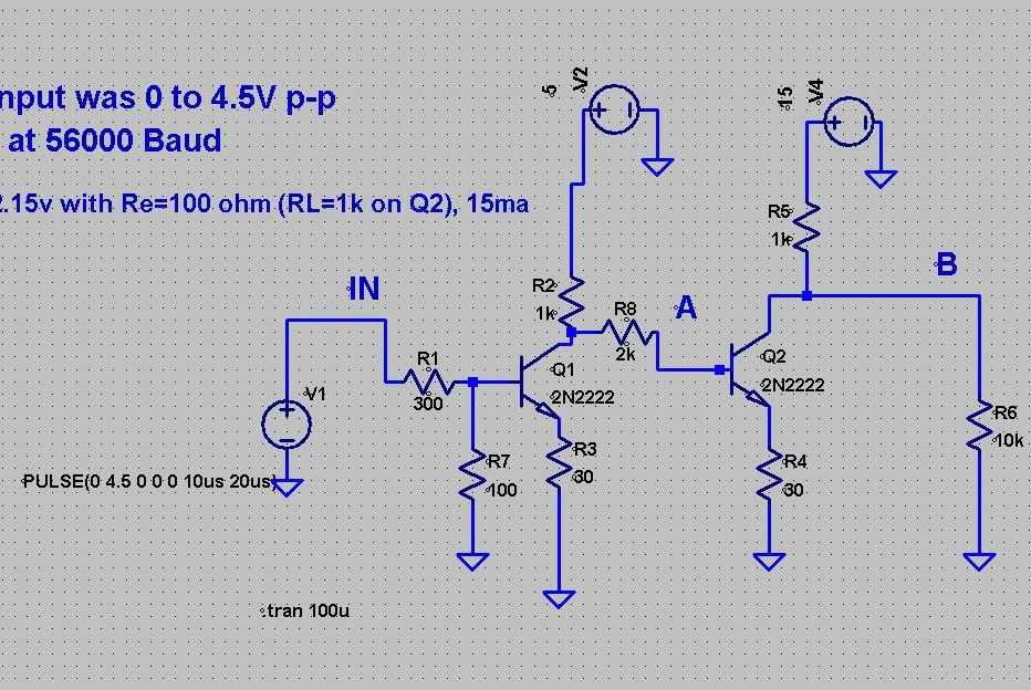
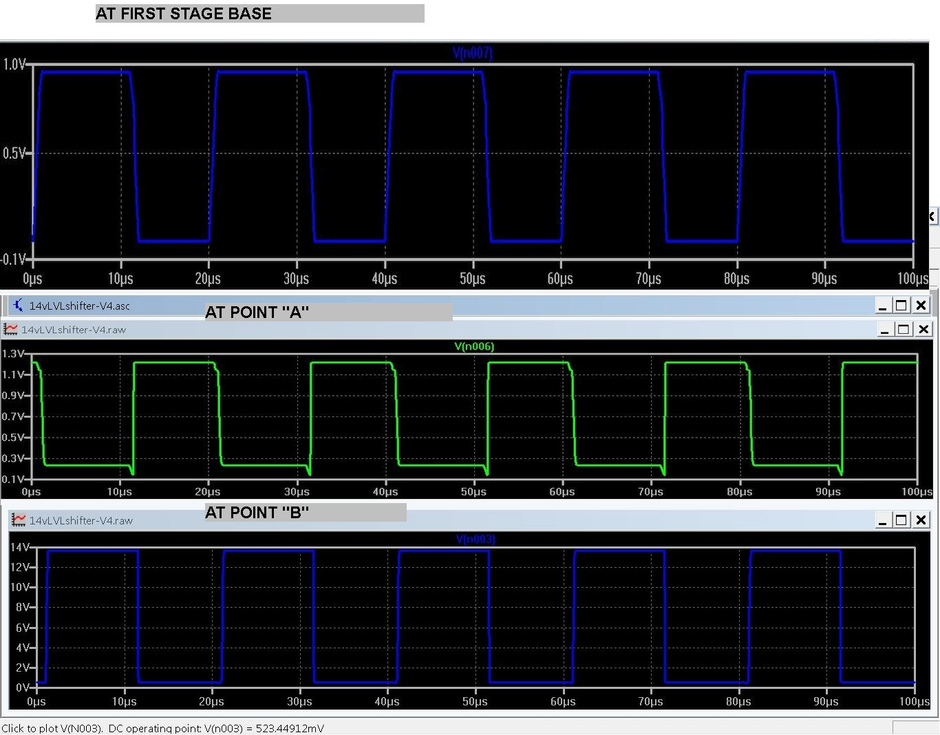
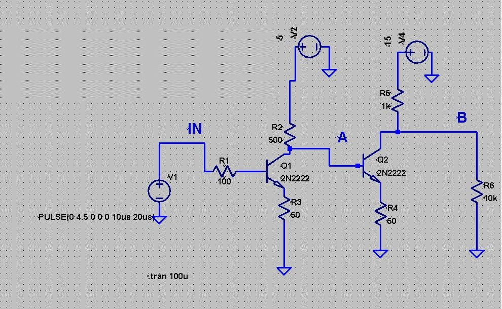
I am designing a simple level translator using 2 transistors connected in series in LTSPICE simulator. I tried with one transistor but the output from the collector pin is 180 degree out of phase, as is usual with common emitter circuit. With 2 transistors, I get this distortion in the lower part of the step in LTSPICE waveform when I attach a probe at point "A" (this would get into stage 2 also.) This goes away when I increase emitter resistor value.

Can anyone tell me the exact reason why the lower part of the step has a hook in it and goes still lower when I try to go lower than 2.25 volts (which I need?) My aim is to go lower on the lower part of the step of the wave to get the "0" to satisfy TTL needs at output of this circuit (under 1 volt.) I don't have any problem in the higher part of the square wave.

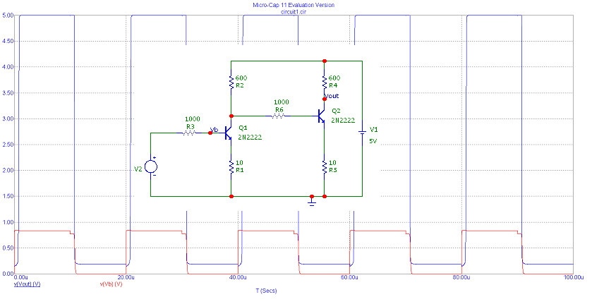
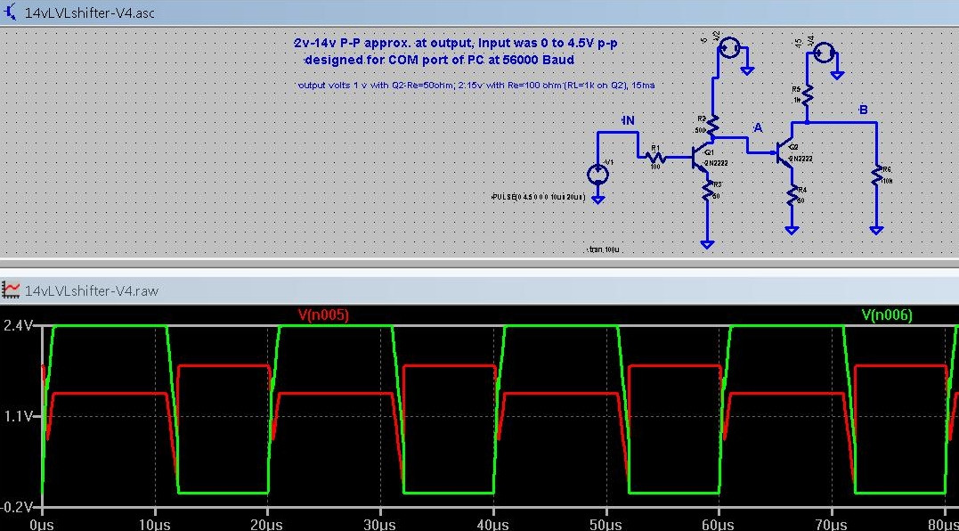
The circuit (first picture), input waveform, output waveform with two different emitter resistors, 300 ohm and 50 ohm. Both are distorted on the "downs." I would like to know the reason!

circuit showing the two waves, at input and output (red is output) the circuit the wave at point "A" shown separately (red)

\$\endgroup\$
5
  • 3
    \$\begingroup\$ Can you please post your circuit and the scope traces showing this distortion? \$\endgroup\$ Commented Feb 7, 2018 at 15:31
  • \$\begingroup\$ I increased R3 (emitter resistor first stage) to 300 ohm from earlier 50 ohm, still the same distortion, I am enclosing LTSPICE waveforms at point A and B (second stage too which shows spikes instead of square wave)! I experimented with placing coupling capacitors of 10mfd in series with each transistor base but no improvement , another form of distortion, hook-like in lower part of step comes in with capacitors. \$\endgroup\$ Commented Feb 7, 2018 at 16:22
  • \$\begingroup\$ @user3048731 What do you expect to drive with this level translator circuit? Does it need to SINK and SOURCE at the output? At what rates? \$\endgroup\$
    – jonk
    Commented Feb 7, 2018 at 16:27
  • \$\begingroup\$ @user3048731 Also, are you aware that LTspice will automatically use something like 10% for the rise and fall times of your input if you don't override it? \$\endgroup\$
    – jonk
    Commented Feb 7, 2018 at 16:30
  • \$\begingroup\$ loose the emitter resistors (use wire instead), and to avoid saturation fit schottky diodes from base to collector. \$\endgroup\$ Commented Feb 7, 2018 at 19:09

5 Answers 5

1
\$\begingroup\$

My aim is to go lower on the lower part of the step of the wave to get the "0" to satisfy TTL needs at output of this circuit (under 1 volt).

The potential problem with the first stage is the value of R1 of 100 ohms. Ignoring the connection of the collector for a minute, think what happens to the actual base voltage when 4.5 volts is at the input to the 100 ohm resistor R1; a potential divider is formed with R1 (100 ohms), the base-emitter (a forward biased diode) and, the emitter resistor (60 ohms).

Current into the base would be approximately: -

(4.5 volts minus 0.7 volts)/(100 ohm plus 60 ohm) = 24 mA.

This current would therefore drop 2.4 volts across R1 and takes the base to 4.5 - 2.4 volts = 2.1 volts. It sounds like an unreal analysis until you start to consider what happens when you reconnect the collector.

The problem is this; the 1st stage collector cannot get below (2.1 volts minus 0.7 volts) because if it did it will also act like a forward biased diode from the base and, the BJT's hFE would be shot to death. So, if the collector starts to get lower than the base, the transistor fails to operate with any respectable characteristics and rapidly turns into two diodes hence my (possibly) rather odd analysis.

Given what I have said, the lowest voltage attainable at the collector is approximately 1.3 volts. Your LTSpice transient response appears to indicate 1.4 volts so I'm not far off with these approximations.

The 2nd BJT stage compounds the problem.

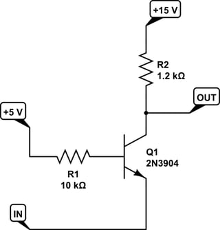
Maybe try this: -

enter image description here

can anyone tell me the exact reason why the lower part of the step has a hook in it

That hook is because the base voltage is rapidly lowering from 4.5 volts back to 0 volts and you reach a point where the collector-base region is not (illegally for a linear amplifier) forward biased anymore. Now the transistor starts to behave with some measure of dignity. At this in-between base level, the transistor is properly amplifying and the collector is being allowed to drop to a voltage that is much less.

\$\endgroup\$
5
  • \$\begingroup\$ Just a note. The base current is more like \$320\:\mu\text{A}\$. You didn't multiply the emitter resistor by beta=200 for the 2N2222 (temporarily assuming active mode.) Or am I missing something? Still a saturated BJT, though. \$\endgroup\$
    – jonk
    Commented Feb 7, 2018 at 16:16
  • 1
    \$\begingroup\$ @jonk, when it saturates the collector/base region goes forward biased and this ruins the hFE. \$\endgroup\$
    – Andy aka
    Commented Feb 7, 2018 at 16:18
  • \$\begingroup\$ Good point. True enough. Need more coffee this AM (it is 8AM now for me.) \$\endgroup\$
    – jonk
    Commented Feb 7, 2018 at 16:18
  • \$\begingroup\$ @jonk it would be worse if the gain remained high - the base would sit even higher and the collector could not drop lower than (say) 3 volts. It's 16:20 for me but getting tired. Who said old age LOL. \$\endgroup\$
    – Andy aka
    Commented Feb 7, 2018 at 16:19
  • \$\begingroup\$ "That hook is because the base voltage is rapidly lowering from 4.5 volts back to 0 volts and you reach a point where the collector-base region is not (illegally for a linear amplifier) forward biased anymore" . @Andy Aka, Thanks a lot, this explains my original question, and for your alternate modified circuit too. About 3 decades ago we had a course in Transistors, so I'm rusty ! Main points I remember are "1) multiply the Re by BETA for input impedance 2) Vbe varies with temperature, stabilise it by a grounding resistor wasting some input current, or with a larger Re 3) Amplific= RL/Re. \$\endgroup\$ Commented Feb 8, 2018 at 4:14
1
\$\begingroup\$

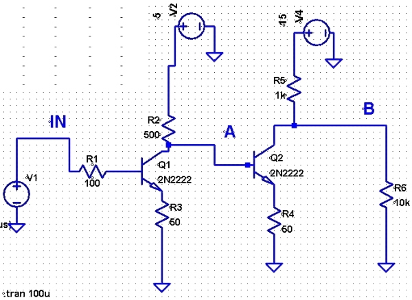
Here is the circuit we are discussing:

If you want the output to go as low possible, lose the emitter resistor R4. Once you do that, you need the input to the second stage to also go low, so lose R3 too.

R2 also seems rather low for what it seems you are trying to do. I'd start with making it about 10x higher, like 4.7 kΩ, for example.

R1 also seems rather low. Especially with R3 gone, such a low value of R1 may load the digital signal too much. Start with making it 1 kΩ or so.

So in summary, make R1 1 kΩ, R2 4.7 kΩ, and short R3 and R4. See how that works.

\$\endgroup\$
1
\$\begingroup\$

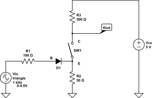
The 'hook' is caused by Base current flowing through the Emitter resistor, which raises the Emitter voltage and prevents the Collector from pulling down to 0V.

To understand how this happens, consider this (grossly) simplified circuit where the transistor is replaced with a diode and switch simulating the Base-Emitter and Collector-Emitter junctions:-
schematic

simulate this circuit – Schematic created using CircuitLab

When Vin rises above ~0.6V the transistor is turned on (SW1 closed) but Vout only goes down to 0.45V because the current flowing through R3 also goes through R2, forming a voltage divider with a ratio of (500+50)/50 = 11:1. This is the condition when there is just enough current going into the Base to turn the transistor on.

The transistor has a high current gain so its Base current is initially very small and does not significantly affect the voltage on R2. However as the input voltage rises it injects more current through D1 into R2, increasing the voltage across R2 and raising the output voltage even higher.

If the value of R1 is increased then current injected into the Base is lower and the 'hooks' get smaller, but Vout can never go below 0.45V. To get the lowest possible output voltage you must reduce R2 to 0Ω. Even then there will still be some voltage drop due to the transistor's internal Emitter resistance, so you should also increase R1 to reduce Base current (it only needs to be a fraction of the Collector current, not 3 times higher!).

Of course a transistor is more than than just a diode and switch, so your waveform has other characteristics that are not explained by this simplified circuit. The transistor amplifies current current linearly so it doesn't turn on and off instantaneously. It also has internal capacitances which slow down the switching action and allow the input to feed through during transitions. This explains why your 'hooks' momentarily reach 0.2V when the input goes low, and don't quite reach 0.45V when the input goes high.

If you reduce the input frequency and increase transition times then capacitive effects are reduced and the output waveform will become more symmetrical. Also note that with Trise and Tfall set to zero LTspice will make the transition times proportional to the total period. To control transition timing you must set Trise and Tfall to specific values.
\$\endgroup\$
1
  • \$\begingroup\$ "The transistor amplifies current current linearly so it doesn't turn on and off instantaneously. It also has internal capacitances which slow down the switching action and allow the input to feed through during transitions. This explains why your 'hooks' momentarily reach 0.2V when the input goes low, and don't quite reach 0.45V when the input goes high. " Excellent advice, explains much to me ! Thanks! \$\endgroup\$ Commented Feb 8, 2018 at 4:07
0
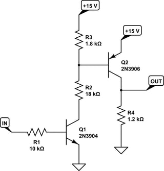
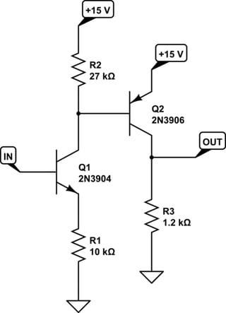
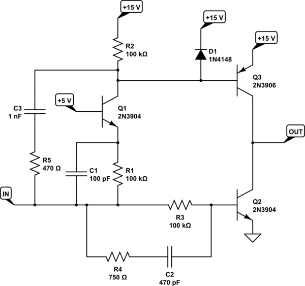
\$\begingroup\$

You already have good answers explaining the bad behavior of your circuit. So I'm not going to belabor that. The job is done as well or better than I could do.

As far as a solution goes, though, that's a different matter.

Your question could use some clarification. Even if you think that you don't need to talk about why, it's still a good idea to explain the reason why you are bothering.

The following answer will explain why it matters.


Circuit 1:

schematic

simulate this circuit – Schematic created using CircuitLab

Circuit 2:

schematic

simulate this circuit

Circuit 3:

schematic

simulate this circuit

Circuit 4:

schematic

simulate this circuit

And there are so many more possibilities.

Please be more specific when asking a question.

\$\endgroup\$
0
\$\begingroup\$

*Thank you for all your answers ! The last one with the detailed circuit works fine ! meantime, i too tried various combinations, and realized the base terminal was probably "overdriven" from your previous answers. here is the modified circuit (was afraid to "lose" the emitter resistor altogether as its popular opinion that some emitter resistor provides "stability" in C-E circuits. so reduced it to 30k. at input it works giving a good square wave with 1K as @Andy Aka suggested in his modified circuit proposal. But it Also works if we bypass some of the current with a base to ground resistor as shown in circuit. Of course this would reduce the input impedance of the circuit, but increase stability. more than 3 decades ago (had more valve radios then) when we did a course in transistors (High School) I remember they told us: "stabilize any transistor circuit by removing effect of Vbe against temperature fluctuations by "wasting" some of the input current to ground with base to ground resistor (upto 10 times x Ib (base current) was recommended back then!), or to use a higher value Re (emitter resistor) (which would appear BETA times larger when seen from Base / input side of circuit) or both! That's old school stuff, don't know if you follow this anymore with modern tolerances on transistors. modified circuitThe wave-forms at each stage - no distortion and going low on the LOWS too to about 0.5 volts to satisfy TTL output levels. The purpose of this circuit is to derive High programming voltage Vpp for a micro-controller. Of course I realise that this circuit cant be used directly, input impedance needs to be checked that it dosen't load the driver.

\$\endgroup\$
1
  • \$\begingroup\$ Even though there is a small "hook" at end of the LOW at output of stage 1 (point "A") in the waveform, it goes away when seen at second stage output (point "B"). \$\endgroup\$ Commented Feb 7, 2018 at 17:33

Your Answer

By clicking “Post Your Answer”, you agree to our terms of service and acknowledge you have read our privacy policy.

Not the answer you're looking for? Browse other questions tagged or ask your own question.