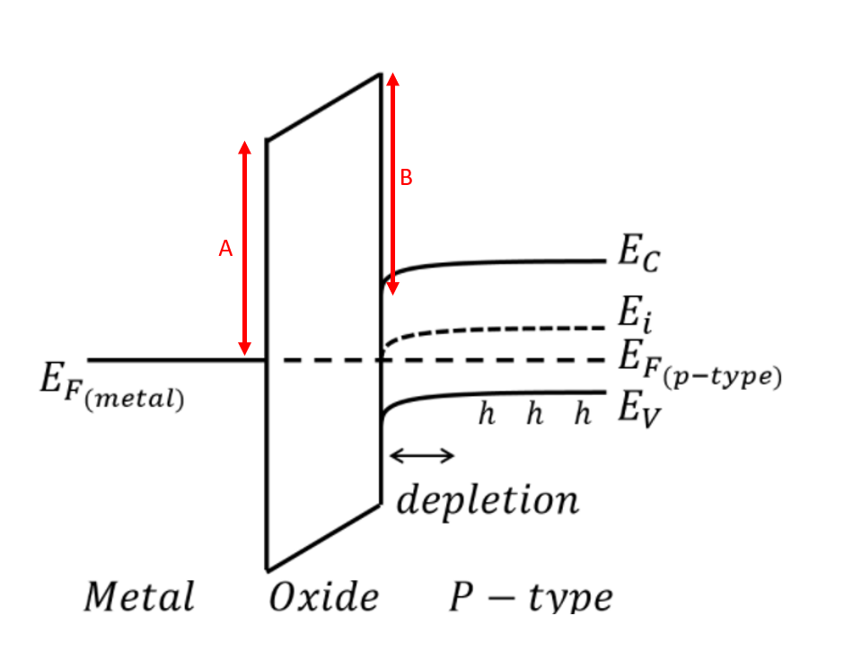
In a MOS system, is the energy offset between metal/oxide or semiconductor/oxide always the same regardless of the gate voltage applied? In other words, are A and B in the diagram above always the same? I think the offset must be always the same since it is determined by the material property (difference between work function of the material), but I see people draw this band diagram under bias as if these offsets change.
1 Answer
A is always the same because it depends only on the metal..oxide work function.i B depends on the accumulation/depletion at the oxide..semconductor interface, so changes (until there is accumulation).
The slope through the oxide changes with applied V, so the amount by which B is above A changes.
In addition, as the V changes, the semiconductor part's depletion region widens, or thins to just an accumulation layer. The curved part in the semiconductor will change with those conditions.
-
\$\begingroup\$ Gotcha, so is B equal to the difference in electron affinity between the oxide and the bulk semiconductor plus the surface potential (amount of total band bending)? \$\endgroup\$ Commented Nov 24, 2021 at 14:44

