3
\$\begingroup\$

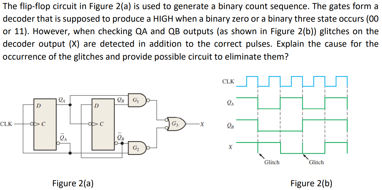
Image showing the question

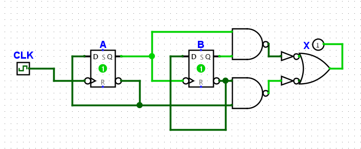
So I have been trying to figure this out. I made the circuit in Logism:The circuit

Though I am having trouble figuring out whats causing it. From what I understand, it could be because 1 of the inputs of the last OR gate (G3) is delayed, and so the output we want changes for that short period.

Here are the timing options I ran the simulation with at 8Hz clk. Timing options

And here is the output Output 1

I changed the gate delay to 1µs and the timing scale to 10µs to enhance the glitches Output 2

I still do not understand what exactly is causing those high and low spikes in the output and how to eliminate it.

Would appriciate if anyone could help.

\$\endgroup\$
6
  • \$\begingroup\$ Note that G3 is just another NAND gate. \$\endgroup\$
    – Dave Tweed
    Commented Mar 12, 2022 at 12:52
  • \$\begingroup\$ We are not going to do your homework for you. If you have a running simulation you should be able to observe all of the signals and figure this out for yourself. \$\endgroup\$ Commented Mar 12, 2022 at 14:20
  • \$\begingroup\$ Put the outputs of ALL the gates in your timing plot, and zoom in on the time scale in the region around one of the glitches. Note how each gate's output changes in turn. Here's a hint: To do this properly, you need to start with the two FFs in a different configuration from the binary counter. \$\endgroup\$
    – Dave Tweed
    Commented Mar 12, 2022 at 14:35
  • \$\begingroup\$ Thanks @DaveTweed, unfortunately logism doesnt allow me to show the flip flops as gates so i can see them live. So I guess i will have manually make the DFF? \$\endgroup\$
    – Crab00189
    Commented Mar 13, 2022 at 7:16
  • \$\begingroup\$ I'm talking about the gates G1 and G2 in the original diagram. You have obviously already realized that their delays have something to do with the problem, since you increased the gate delays to "enhance the glitches". Now take a closer look at what they're actually doing. Note that "gate delay" also refers to the clock-to-output delay of the DFFs. \$\endgroup\$
    – Dave Tweed
    Commented Mar 13, 2022 at 11:29

1 Answer 1

3
\$\begingroup\$

This is your homework/coursework, so this is to guide you, not to supply the answer. This information is all available on the internet.

You can see from the timing diagram that the X glitches occur when the outputs of DFF_A and DFF_B both change level, on the same clock edge.

You can then follow through the effect on the gates that DFF_A and DFF_B drive.

Remember that the model you have is trying to model real circuits as best it can. In real digital circuitry, the two DFF outputs will not change literally simultaneously from the same clock. There will be slightly different responses from each circuit, different propagation delays along the connection in and out of the DFFs etc. Models either ignore these delays completely or try to emphasise them by showing large glitches. Here, your combinatorial gate settling time shows the uncertainty in the outputs as both DFF outputs change across each other, one rising and one falling.

Glitches in combinatorial logic circuits are unwanted transient output states. They are caused when the inputs are at intermediate states before reaching their final states.

They are removed by:

  • Not having any unwanted input combinations. For example, by only having a single input change at any time and only from its previous level to a new final level.

  • By filtering the output. In synchronous logic circuits, this is usually by passing glitchy outputs through a further DFF. But this introduces a delay in the output of up to 1 clock so it may not be allowable.

You will have to think through this information and your circuit to find the solutions, explain them and justify them.
\$\endgroup\$

Your Answer

By clicking “Post Your Answer”, you agree to our terms of service and acknowledge you have read our privacy policy.

Not the answer you're looking for? Browse other questions tagged or ask your own question.