I'm using an AS6C1008 SRAM chip, and I'm having an odd issue with it. The voltage supply going to this chip is created from a stiff 5V supply (VDD) and a 3V backup battery (CR2032), diode or-ed together (calling this net VCC). During normal operation (powered by VDD), measuring with an oscilloscope and also verifying with a multimeter, I see the voltage supply on VCC raise up usually to about 5.6V. Sometimes, I have seen voltages as high as 5.8V. This only occurs when /CS1 is at VCC for a long enough period of time - as /CS1 is pulled to GND, the VCC supply will discharge, eventually reaching to VDD minus a small diode drop, as would be expected. Once /CS1 is returned to VCC and the SRAM is no longer enabled, VCC will charge back up to ~5.6V.
And to add to the weirdness, using the similar but smaller AS6C62256 SRAM chip doesn't exhibit this behavior. VCC is equal to VDD minus a small diode drop as would be expected.
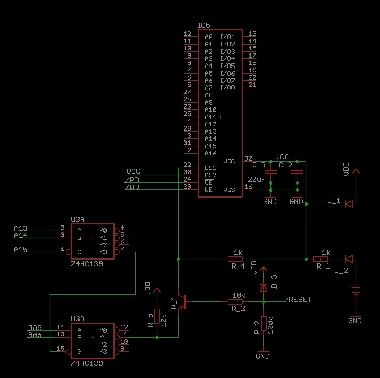
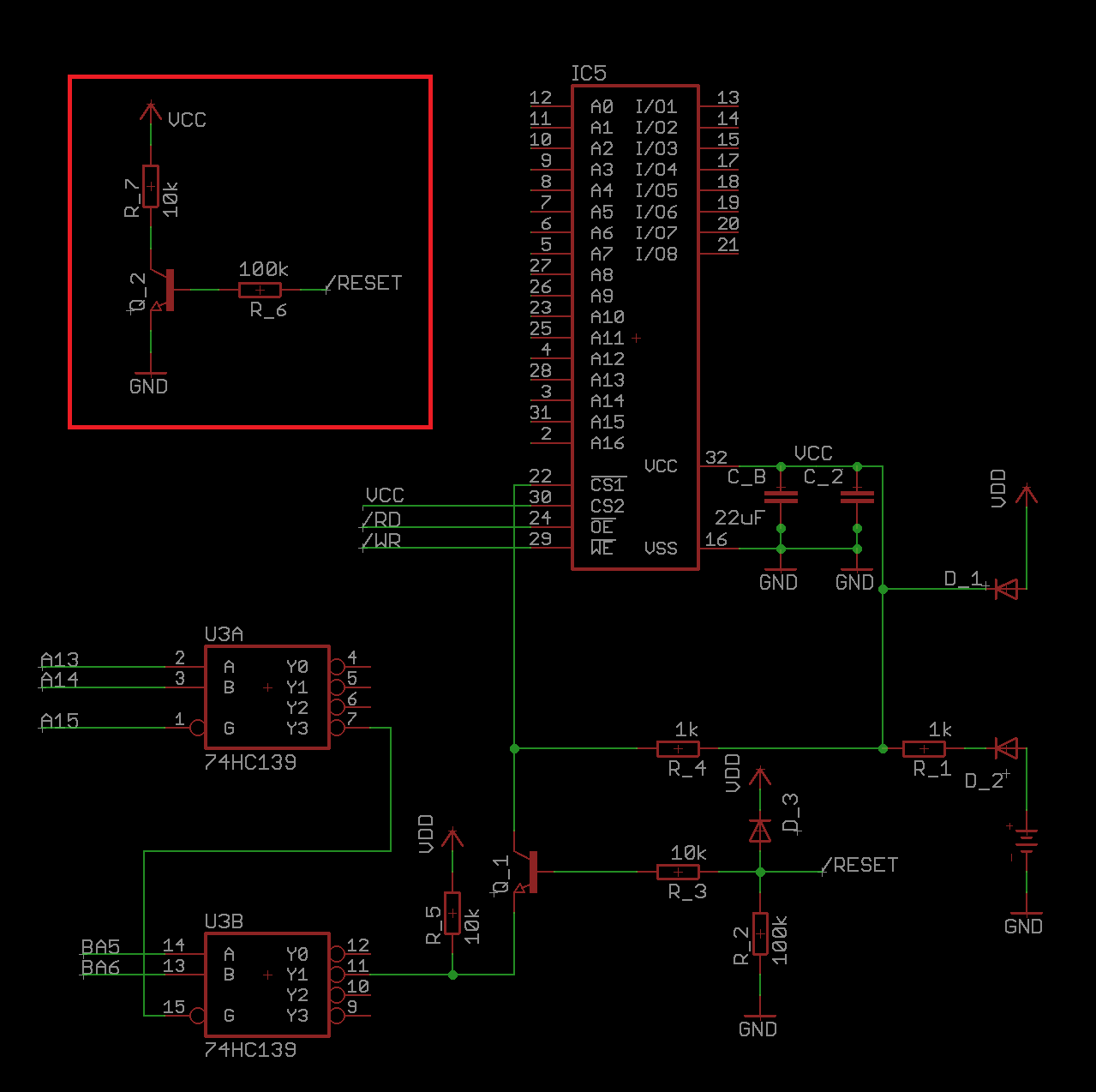
Circuit
Using a 62256 (28-pin device) in place of the 1008 (32-pin device) works because the supply pin is tied to VCC in either case. (Originally, A15 and A16 went to actual address lines, but I ended up tying them to GND for testing so it mimics a 62256)
Definitions and Parts
VDD: 5V supply, VCC: diode-ored voltage from VDD and battery. All address/control pins on the SRAM (IC5) are referenced to VDD, except /CS1 and CS2 which are referenced to VCC. /CS1 is called CE# and CS2 is called CE2 in the datasheet for the AS6C1008.
Q1 is a 2N3904, D1-D3 are BAT85 Schottky diodes, CB is a 22uF alel, C2 is a 100nF ceramic bypass cap (both are located very close to the SRAM chip). /RESET net is GND when VDD is off, otherwise it's ~VDD (for the purposes of this operation, /RESET is always logic HIGH)
Operation
When a specific address range is accessed (A13, A14, etc.; max clock speed is ~4MHz), the 74HC139 will pull the Y1 output low. /RESET is HIGH, so current flows from collector to emitter of Q1, pulling /CS1 LOW. When the specific address range is not being accessed, Y1 is HIGH, and /CS1 is HIGH. CS2 is always set to VCC, allowing CE# to control access to the RAM (and maintain low standby current when VDD is removed).
I cannot change the VDD supply or the clock speed, these lines are external to my board.
Scope Traces
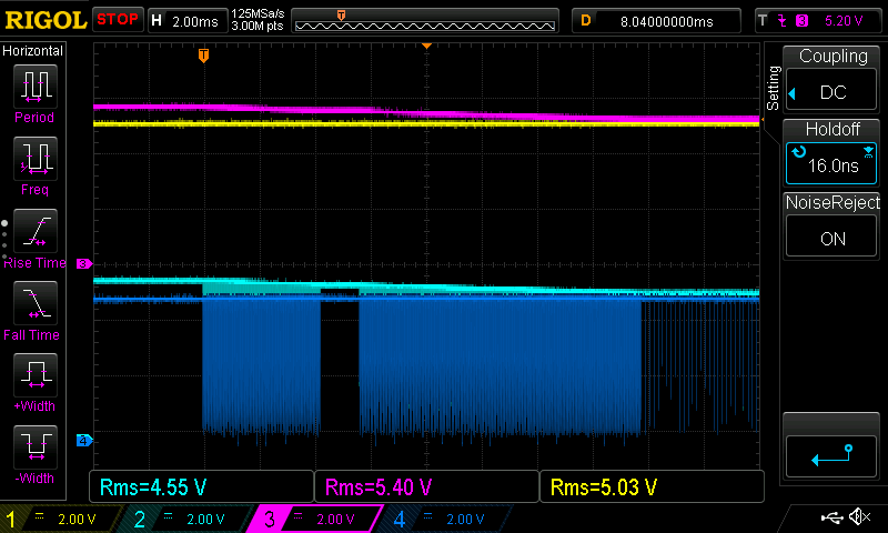
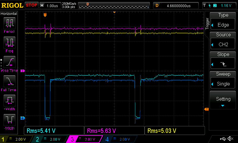
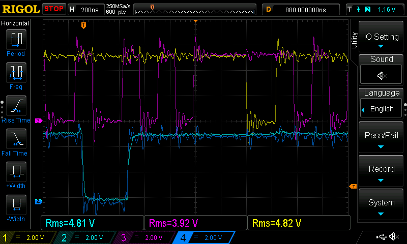
Ch1 (yellow): VDD, Ch2 (light blue): /CS1, Ch3 (purple): VCC, Ch4 (dark blue): Y1 output of 74HC139. These traces are measured with the reference directly on the GND pin of the SRAM chip, but the GND reference is the same everywhere on the PCB with thick traces/planes.
In the first capture, VCC starts at around 5.6V. At the trigger (set at 4ms from left side of capture) the SRAM begins to be accessed by pulling /CS1 LOW. As this addressing continues, VCC keeps discharging down, until eventually it reaches VDD (convergence is off-screen).
The second capture is zoomed in at the first pulses of /CS1. You can see that after a ~0.5us pulse of /CS1, the voltage returns to VDD, not the higher VCC, for about 1us before returning to 5.6V. As time goes on, /CS1 begins to match Y1 output because VCC lowers to ~VDD.
EDIT: Ch1 (yellow) is /WE and Ch3 (purple) is /OE.
Attempted (and Failed) Solutions and/or Troubleshooting Steps
Doing the following barely impacted the increased voltage, if at all:
- Tried three separate 1008 chips
- Changed values of R3, R4, and R5 (100k, 10k, 10k; 100k, 33k, 33k; etc.)
- Removed R1 completely to remove the battery from the equation
- Swapped out the BAT85s for 1N4148s
- Removed CB and C2
- Added series resistance of about 50Ω to the SRAM supply
- Added 1Mohm across VCC to GND
- Tied pin 1 of the AS6C1008 (which is NC) to GND, VCC, left floating (it was a shot in the dark)
Solutions That Worked (But I Don't Want)
- Small series resistance + 5.1V Zener diode in parallel with supply pins, but this greatly increases (~30x) the current out of the backup battery when VDD is removed
- Adding a 100k across VCC to GND fixes it, but as with the zener, causes the battery to drain faster.
- As mentioned, replacing the AS6C1008 with an AS6C62256 fixes the issue, but I also only get 25% of the available SRAM memory
- The AS6C6264 also doesn't exhibit this issue either
So... it kind of seems like I somehow made an unintentional charge pump. But I'm not sure how, or why, especially that it only affects the 1008 and not the 62256 or 6264. Does anyone have any ideas of how to mitigate this without sacrificing battery life from the backup battery?
EDIT: Potential Solution
I decided to add another NPN that will turn on during normal operation (/RESET is at VDD) to load VCC with a 10k resistor. When /RESET is low, Q2 shuts off and allows minimal leakage current (measured ~0.5uA). This way, I can put VCC at the expected safe value, while not impacting battery life with a constant load. This doesn't tell me why VCC is raising up above VDD in the first place without a load, but this does seem to fix the symptoms.
Originally I tried tying R6 to VDD instead, but there is some leakage current through D1 that allows VCC to charge up the bulk capacitance on VDD (not shown in schematic) to about 0.5V. This will bias Q2 enough to allow some current through R7 (measured ~10uA).
EDIT: Alliance Repsonse
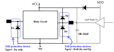
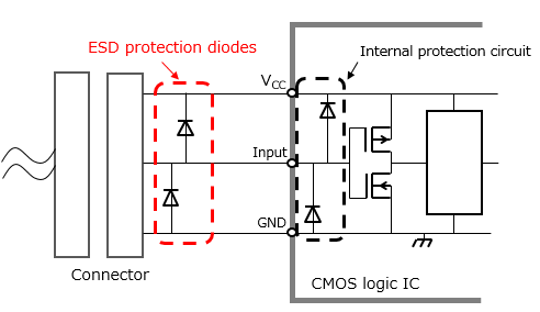
Thankfully, Alliance actually got back to me. It appears that the 1008 SRAM chips have an extra ESD protection diode included from the input to VCC (Dp in the schematic). The other series of chips do not have these diodes, only using the one from the input to GND (Dn).
So it looks like the input noise is being rectified into the supply, and not being discharged fast enough. I think I will stick with the NPN circuit I've added to lightly load the supply while power is on to keep VCC at proper levels. Shortening/thickening the traces isn't extremely feasible, and adding series resistances to dampen the noise would greatly increase the BOM count, and I probably don't have enough room for them anyway.

