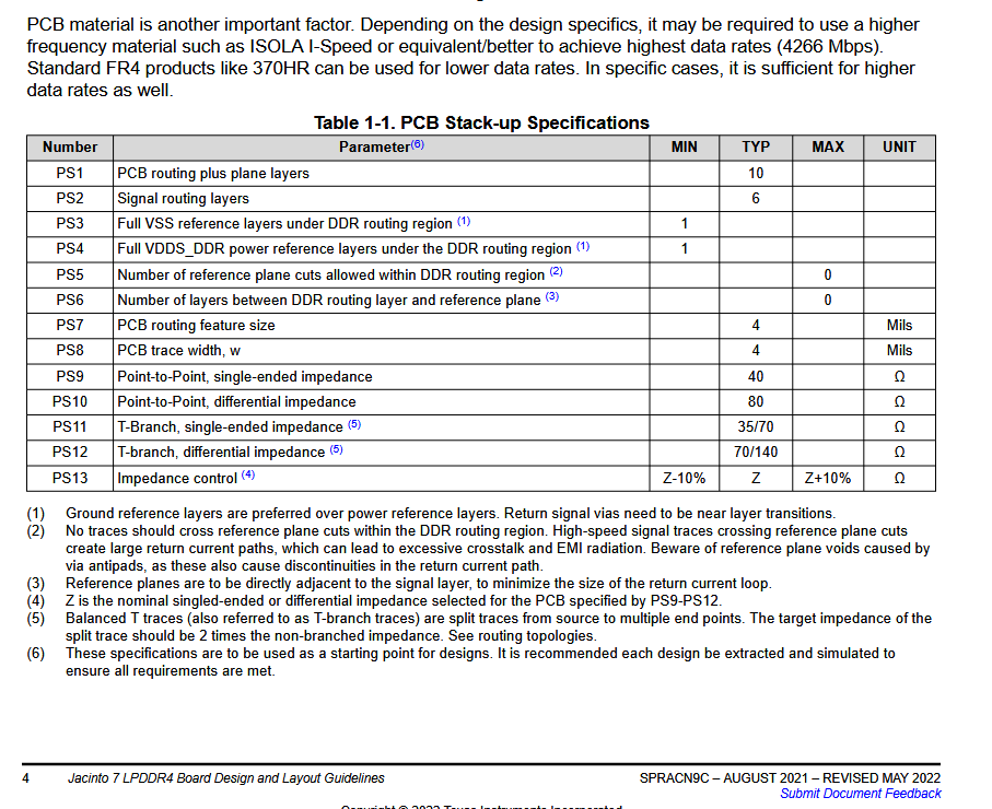
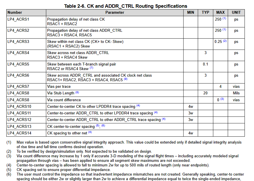
are all the signals to be routed with 50Ω impedance?
Maybe but NO, that is not sufficient to ensure adequate eye margin. It is important to get the scattering parameter (s-parms) from both the DDR supplier and uC or SoC supplier to guarantee impedance matching for both LVDS (95ohm) and DDR signals. The board dielectric choices affect insertion loss, loss tangent @ f, and slew rate and may contribute to edge dispersion and eye window margin loss. It is important to create a budget for each contribution to eye window (EW) margin loss.
The design rules are available from many suppliers incl; TI NXP Micron The board shop must verify the integrity of all traces with specified impedances using TDR "electrical tests" on your PO to your design specs.
You need to collect all device s-parms and material and design data to prevent impedance discontinuities, skew jitter, margin loss, dielectric loss skew, surface roughness skew, trace and via crosstalk, effects on inter-symbol interference (ISI) from frequency-dependent impedance, stub interference, match microstrip, stripline, and coplanar stripline impedances and run TDR and eye pattern simulations.
e.g. from TI


PCB design and material choices are critical at these frequencies because 50 Ohms is not 50 Ohms at all frequencies and can vary from 1mm to the next if there is less glass in the weave when parallel to the weave. RF signals travel through PCB material, and will experience loss and distortion due to Dk & Df, skin effect with a surface roughness of copper foil. For digital signals, this results in attenuation, pulse broadening, timing errors, and loss of window eye (WE) margin.
disclaimer:
This is the approach I would initiate if given the task to design with this technology to achieve low error rates and high window margin.
Also, review the web for existing 3rd party designs with revisions.
e.g. https://www.96boards.org/documentation/consumer/aiml/hardware-docs/files/aiml-sch.pdf


