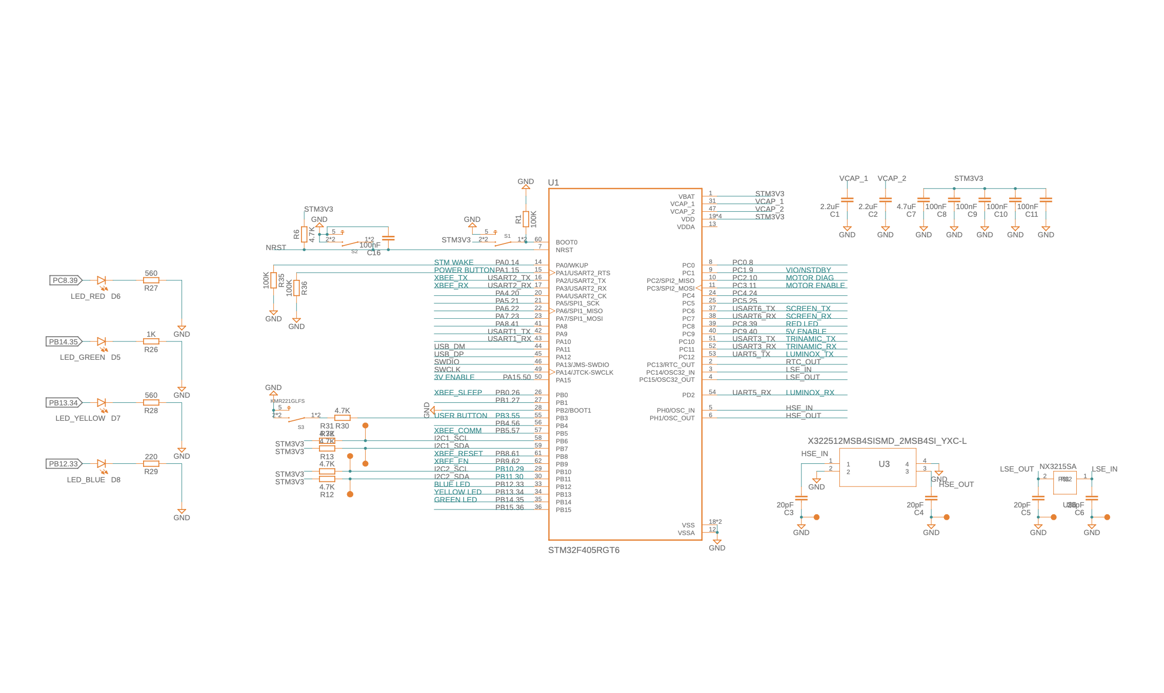
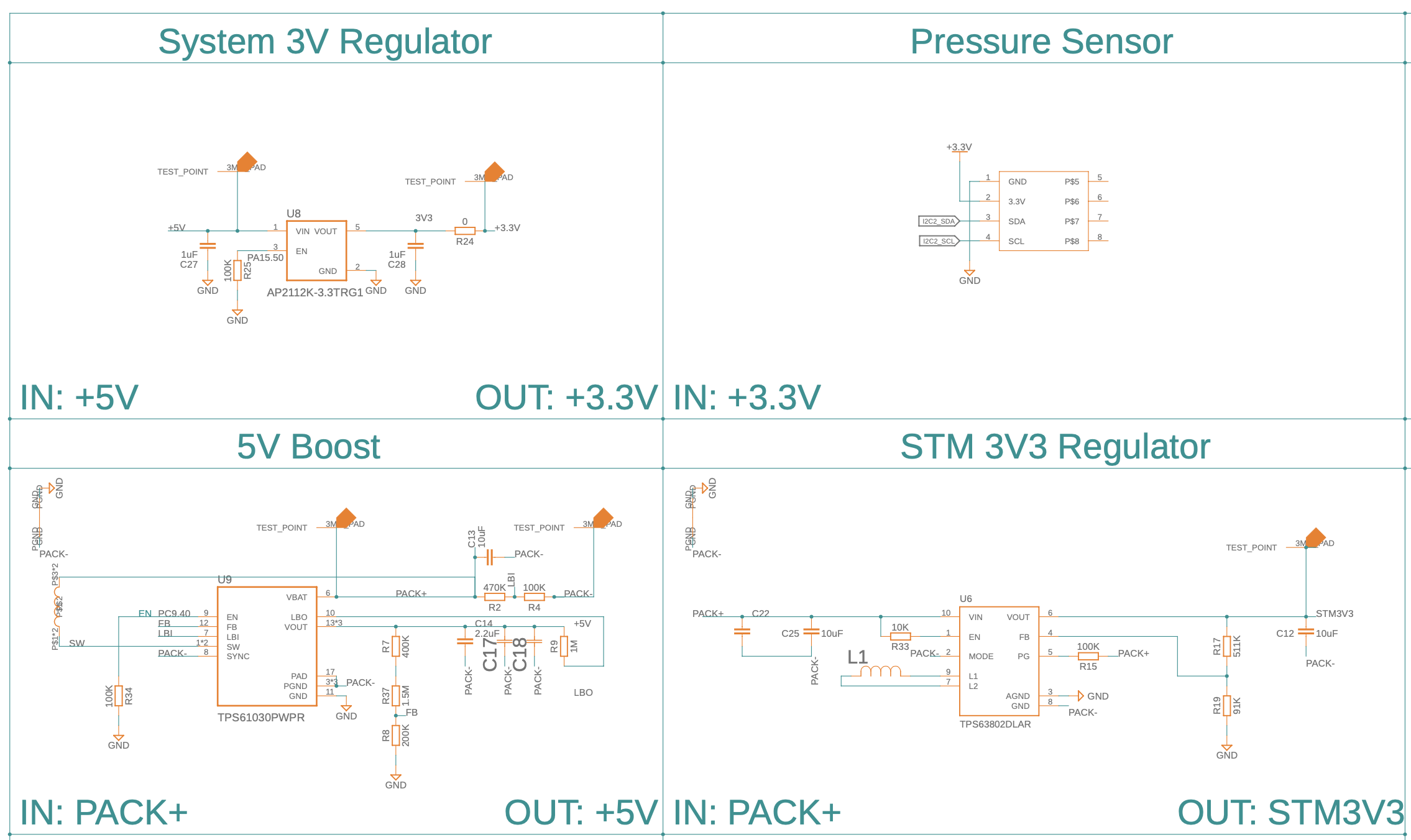
The device I'm designing consists of an STM32F405, a few 3V peripherals, and a few 5V peripherals. The device is is powered off of a 12700 Li-ion battery. The first regulator is a buck/boost that is directly connected to the input of the battery and feeds the STM, the idea is that the STM is always powered and is in deep sleep until a button wakes it up. There is then a 5V boost switching regulator and another 3V LDO that both have their enables on the STM GPIO, these two are in series so the 5V has to be enabled first in order to turn on the 3V LDO. This setup is niche and I think there is something to learn from the problems that I am having. Keep in mind the STM powered by the first 3V regulator is pulling up all of the I2C lines of the peripheral that is powered on a separate 3V bus.
The problem I'm seeing is that the system 3V LDO output without being enabled has a floating voltage on its output. Is this because the isolated regulators share a common ground, and are technically being used on the same devices because of the I2C pull-ups? Also, with the system 3V regulator not populated and 5V is applied to PACK+ I get 5V if I measure between PACK+ and 3V, why is it grounding through 3V?


