3
\$\begingroup\$

I recently designed an H-bridge circuit to try to develop a wireless charging circuit. I am currently generating the PWN signals with a function generator.

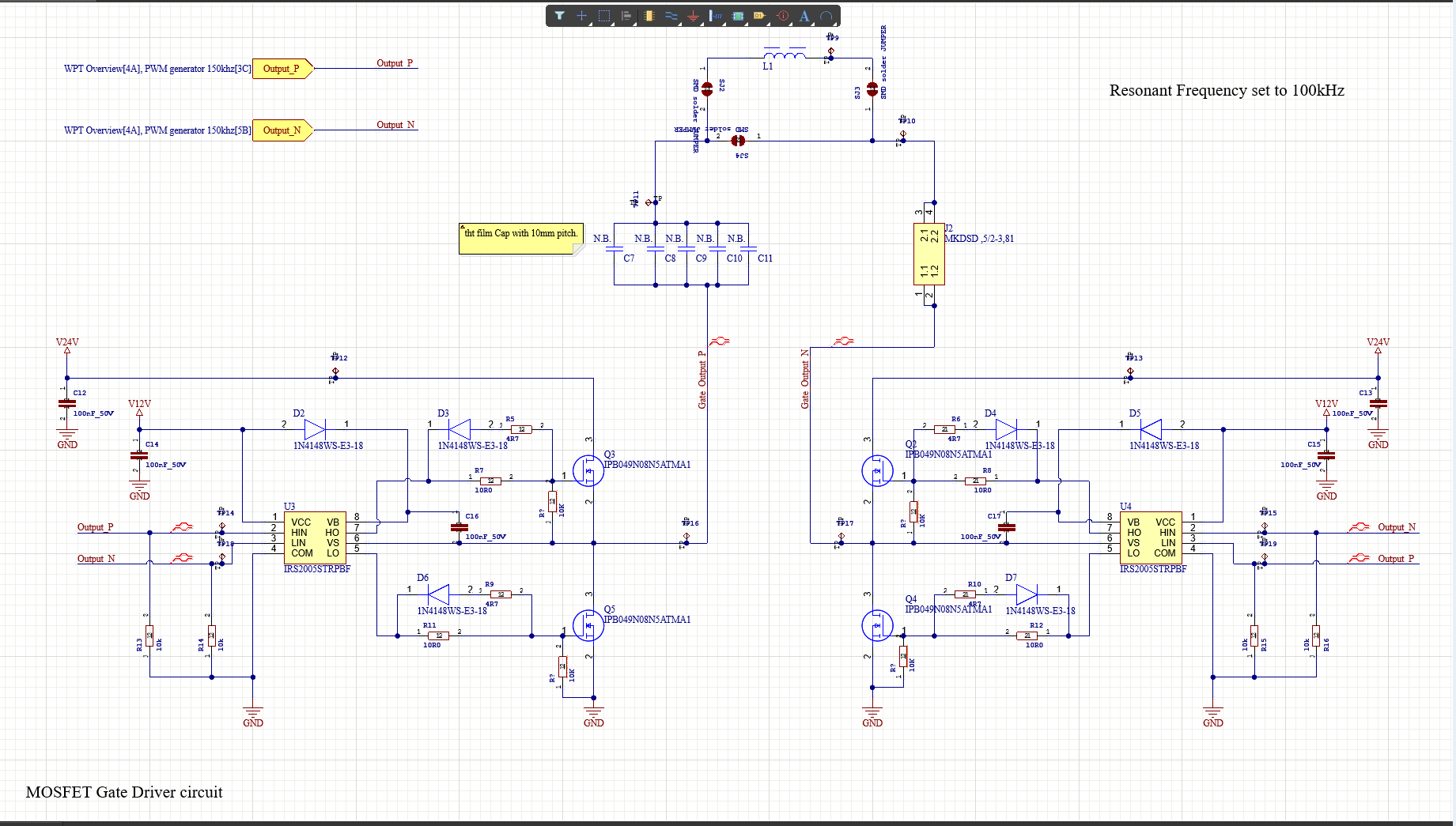
There are two signals which are at 10 Vp-p at 100 kHz with a 50% duty cycle. These signals are driving two MOSFET drivers (IRS2005SPBF). These drivers are connected to 2 N-channel MOSFETs (IPB049N08N5). The subsequent circuit is made up of an LC circuit which provides the resonance for the coil.

The issue: The circuit was not working, and the power supply indicated that there was a large amount of current flowing which might indicate a short circuit somewhere. I removed two MOSFETs and then the circuit worked.

Both drivers would only output the LO signal. Adding a 10 kΩ gate resistor to the circuit subsequently solved that issue (this is still with the 2 MOSFETs removed).

I currently can see the output of the MOSFET drivers at the input to the MOSFETs. When I soldered the 2 MOSFETs back to the circuit, I had the same issue I had at the beginning. I am not exactly sure where I went wrong. My schematic is based on the 200 W development kit from Würth.

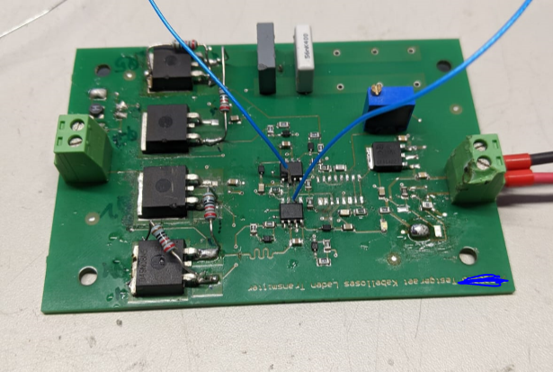
The circuit also has a 24 V to 12 V voltage regulator, and a TL494 PWM generator which has been removed for the sake of testing. The two blue wires connected to the MOSFET drivers are from the function generator and hence soldered to the input wires of the MOSFET drivers.

enter image description here

enter image description here

The schematic is of the gate driver circuit, and the PCB with the added resistor soldered directly to the board.

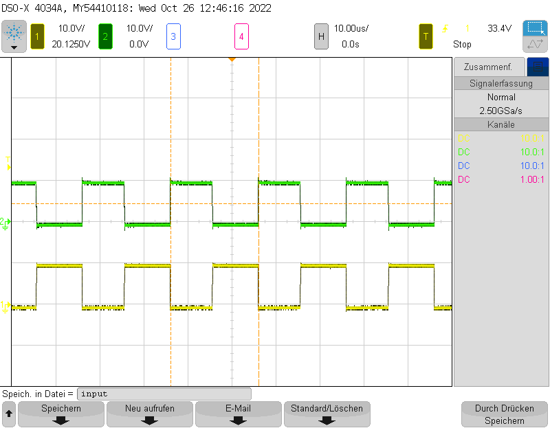
Edit1: enter image description here This is the input waveform that is being given to the two mosfet drivers as a HIN and LIN
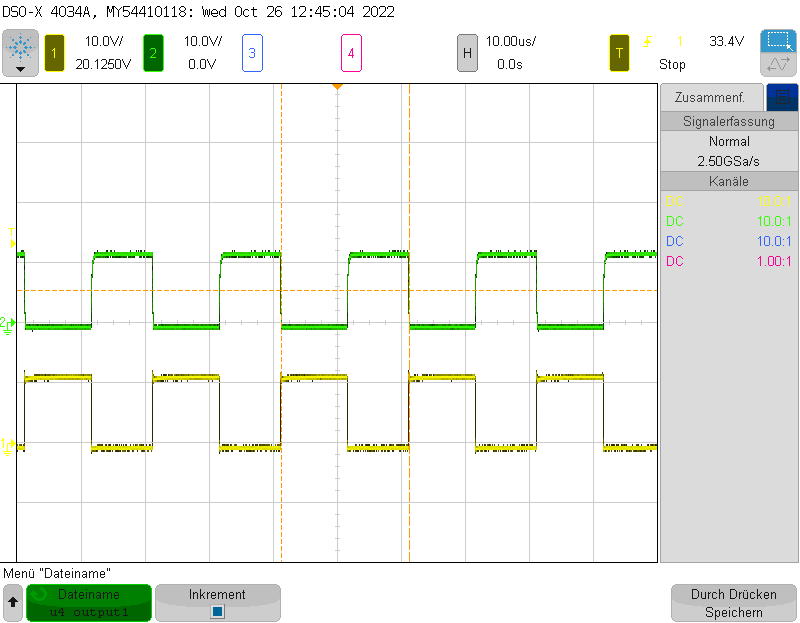
enter image description here The output waveform at mosfet driver U4, the driver on the right.
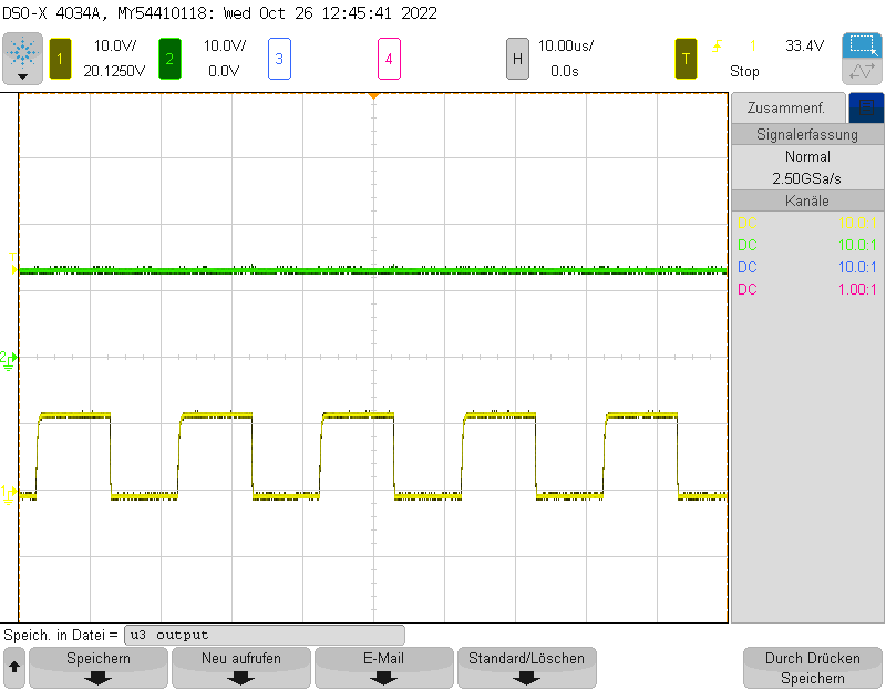
enter image description here The output waveform of the mosfet driver u3, the driver on the left. For some reason Q3 or the top left mosfet doesnt seem to show any switching now. hence the constant voltage ~12v.

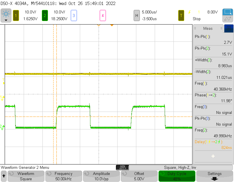
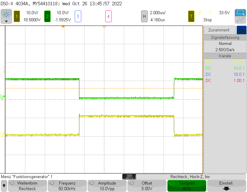
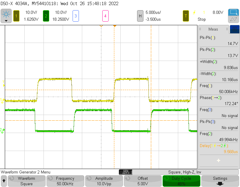
Edit 2: enter image description here This is the HIN and LIN input zoomed in. 48% duty cycle, reduced the frequency to 50kHz But as pointed out, this does not have a dead time.
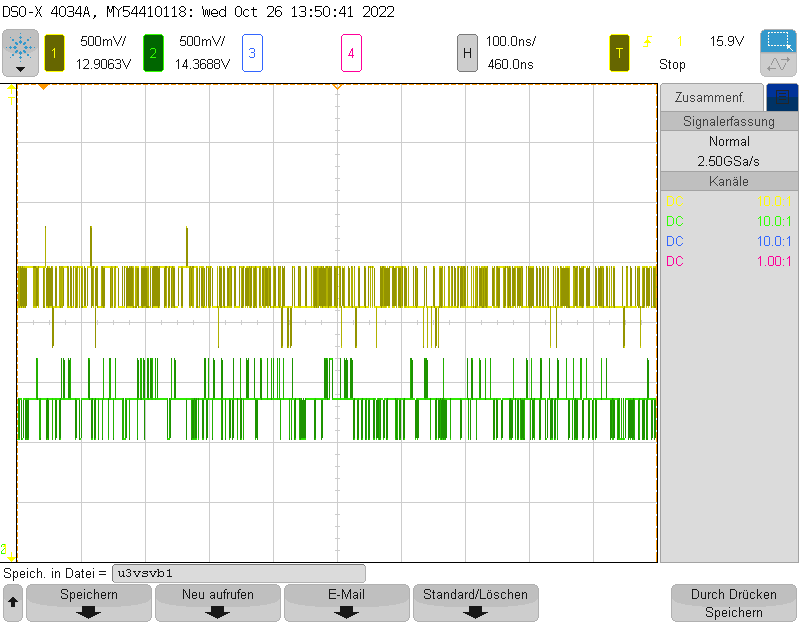
enter image description here This is the VB VS output waveforms. VB-> Yellow, Vs-> Green
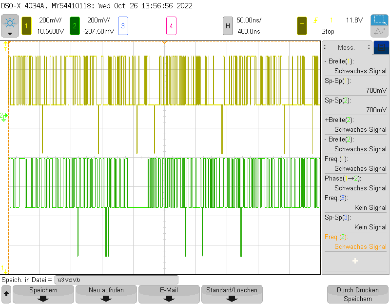
enter image description here This is the VB and VS output waveforms. VB-> Yellow, Vs-> Green

Edit 3: I changed the Mosfet driver from IRS2005 to the IRS2108. enter image description here
This is the measurement taken at the outputs of the mosfet driver U4(to the right of the schematic). There seems to be small amount of dead time there added from the mosfet driver.

enter image description here

This is the output from the mosfet driver u3.(To the left. The mosfet Q3 or the one connected to the 24V supply is stuck high. while the 2nd mosfet Q5 has the switching input from the mosfet driver)

Still Not sure why the mosfet is stuck high. is it due to the Rgs resistor or need for a bigger boot capacitor?

\$\endgroup\$
6
  • \$\begingroup\$ What Vboot voltage do you measure with regards to Vs? Is your bootstrap diode fast enough and can take the voltage? Is your bootstrap capacitor large enough? How does startup of the circuit look? Do you have any soft start ramp? Do you have any deadtime between HIN and LIN? If not (a true 50/50), you will have shoot through current. Please post oscillograms. \$\endgroup\$
    – winny
    Commented Oct 26, 2022 at 9:11
  • \$\begingroup\$ The Voltage at Vs for mosfet driver U4 is ~12V while the voltage at U3 is 0V. i changed the capacitor value from 100nF to 330nF. I currently do not have a dead time with this input from the function generator. but changed the duty to 48%, but i guess thats not the same. \$\endgroup\$ Commented Oct 26, 2022 at 10:10
  • \$\begingroup\$ No, it's not the same @EmeraldMonk \$\endgroup\$
    – Andy aka
    Commented Oct 26, 2022 at 10:28
  • \$\begingroup\$ Please zoom in (in time) on the crossing between HIN and LIN. \$\endgroup\$
    – winny
    Commented Oct 26, 2022 at 10:49
  • 1
    \$\begingroup\$ Thanks, but I can't tell the DC levels of each. I'm not used to Aglient though. As pointed out, you need to add a deadband between HO and LO of about 100 ns or more. \$\endgroup\$
    – winny
    Commented Oct 26, 2022 at 11:26

2 Answers 2

3
\$\begingroup\$

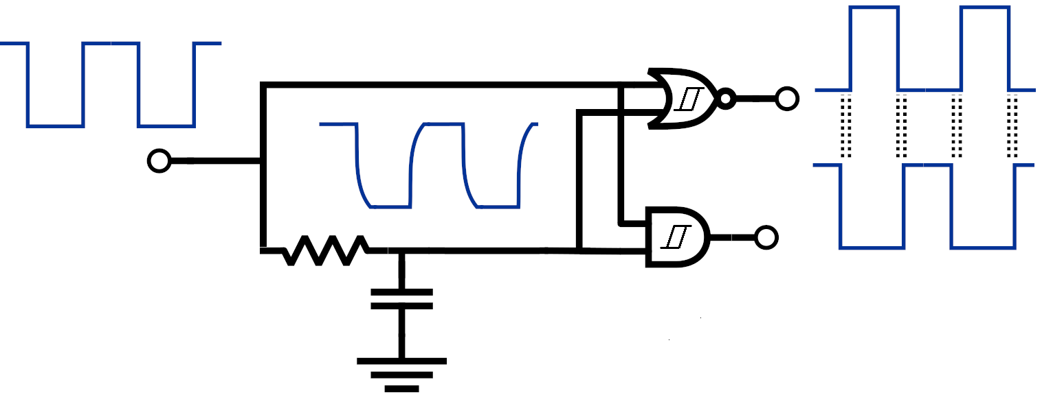
"Shoot-through" is a name given to the simultaneous or over-lapping conduction of both MOSFETs in a half-bridge circuit. To avoid this we leave several tens of nanoseconds gap between deactivating the lower MOSFET and activating the upper MOSFET then, perform the same ritual when deactivating the upper MOSFET and re-activating the lower MOSFET for each half-bridge.

Of course, this is made easy by buying/using MOSFET drivers that have anti-shoot-through circuits built in like this: -

enter image description here

However, your MOSFET drivers don't have anti-shoot-through avoidance circuits and, you appear to be driving both MOSFETS without any care in this respect. This will produce large surge currents in your power supply.

Image taken from here and here.

\$\endgroup\$
13
  • \$\begingroup\$ This makes total sense. I have another mosfet driver kicking around -> [IRS2108SPBF ](infineon.com/dgdl/…) this has cross conduction prevention logic. would help with the anti-shoot through circuit? \$\endgroup\$ Commented Oct 26, 2022 at 10:25
  • \$\begingroup\$ I expect it will help greatly @EmeraldMonk \$\endgroup\$
    – Andy aka
    Commented Oct 26, 2022 at 10:26
  • \$\begingroup\$ What would you recommend to be an appropriate dead time for the respective PWM waves. 50ns? \$\endgroup\$ Commented Oct 26, 2022 at 11:23
  • \$\begingroup\$ Try it and see what happens. It's hard to make recommendations without simulating but, 50 ns sounds about the right ballpark @EmeraldMonk \$\endgroup\$
    – Andy aka
    Commented Oct 26, 2022 at 11:28
  • 1
    \$\begingroup\$ At perfect resonance the series L and C act like a short circuit so, maybe you need to control the duty cycle of your input PWM so that it is much smaller @EmeraldMonk <-- you could achieve the same by lowering the 24 volt DC supply to something much lower then building it up gradually to see what happens. \$\endgroup\$
    – Andy aka
    Commented Oct 27, 2022 at 15:06
2
\$\begingroup\$

Thank you for the Help, I found out that the footprint of the MOSFET was wrong. By this i mean that the Source and the drain were interchanged. This caused the wrong signals//voltages being inputted to the wrong pins hence causing the short circuit. I would like to point out the advice from @Andy aka, and @winny helped me to understand the circuit more and prompted me to change the MOSFET driver which also the wrong one chosen by me. Changing it to the new MOSFET Driver and making the changes to the PCB has made the circuit work enough for me to continue with further tests.

\$\endgroup\$

Your Answer

By clicking “Post Your Answer”, you agree to our terms of service and acknowledge you have read our privacy policy.

Not the answer you're looking for? Browse other questions tagged or ask your own question.