1
\$\begingroup\$

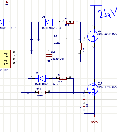
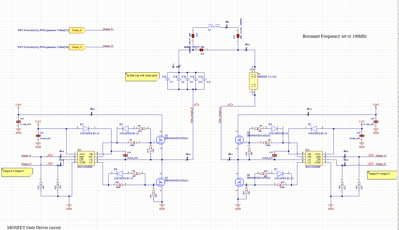
I have 4 N-channel MOSFETs connected in a bootstrap configuration with an IRS2108 MOSFET driver. Currently, only the low-side output works with this circuit. I am not sure why that is.

enter image description here

The schematic depicts a different MOSFET driver, it was changed to the one mentioned above.

Test condition: I put a 40 % duty cycle, 10 Vp-p square wave input on Hin and Lin. For the output I can only measure the LO signals from both the MOSFET drivers. No Ho output.

There is about 500 ns dead-time introduced in the signals by the MOSFET driver. I have changed the bootstrap capacitor to 330 nF, 50 V and the capacitor for the MOSFET driver VCC has also been changed to 4.7 µF.

Any help or guidance is welcome.

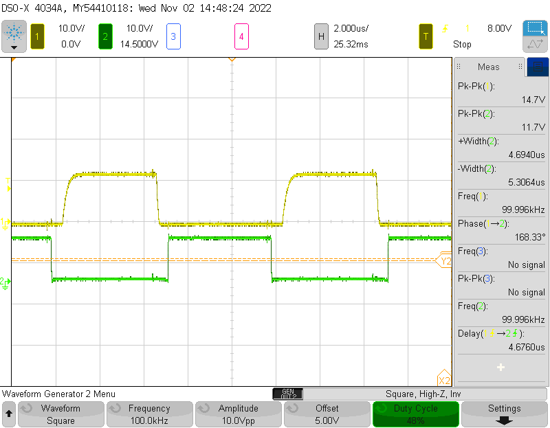
Edit 2: I made the test as stated by @rohat Kilic. (Removed the Hhgh side MOSFET and left the resistor between source and gate of the high side MOSFET.) With MOSFETS Q4 and Q5 still on the PCB, I have this waveform:

enter image description here

Yellow is the HO, and Green is the LO of the LEFT hand side of the schematic.

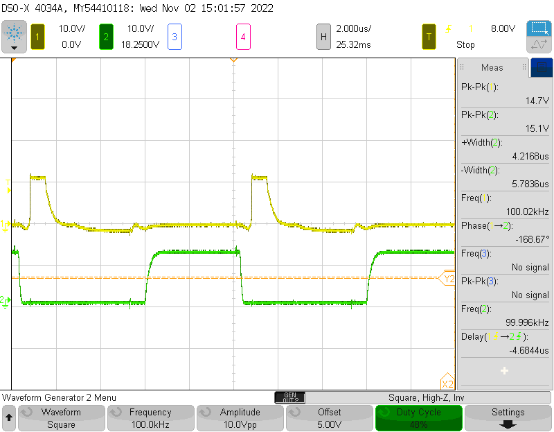
The waveform of the right hand side which includes the MOSFETs Q2 and Q4 is as below.

enter image description here

Yellow is the LO and green is the HO. Ho is different in this case. which means something to do with the bootstrap capacitor? I replaced it but still have the same output.

Tested with 100 kHz. Circuit doesn't want to work when all MOSFETS are soldered to the board.

Edit 2: Blue: HO Green: LO Yellow: Vs all referenced to ground enter image description here
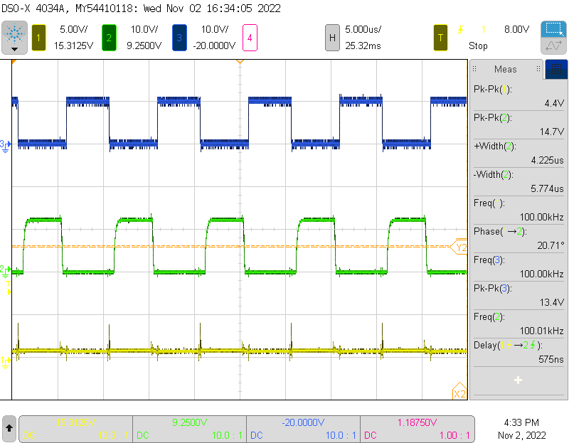
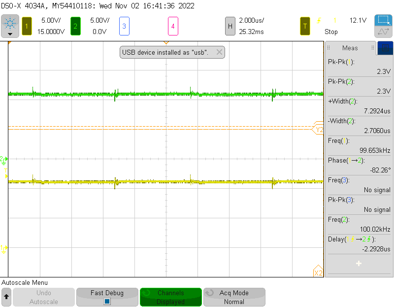
Edit 3: Vboot waveform of the two MOSFET drivers. Green: The one the right Yellow: The one on the left I have no clue if this is how it should be. Referenced to ground.

enter image description here

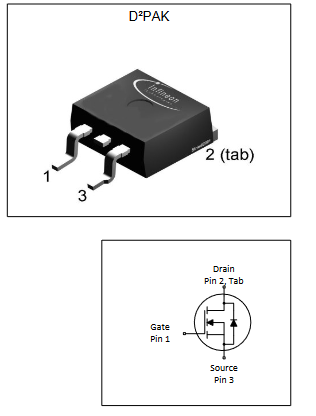
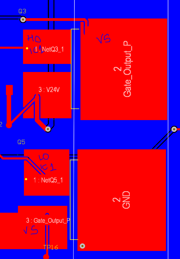
Edit 4: I noticed a that the numbering of the source and the drain in the schematics and that given in the datasheet are different.

enter image description hereenter image description here

I need a new pair of eyes because i think this might be the cause of my issue, but the more I compare it with the layout in my PCB design, I feel like there is nothing wrong. But for sure the numbering is an issue.

enter image description here

This is a clip from the PCB of the two MOSFETS Q3 and Q5 that are connected to IC1.

Edit 5:

The Footprint of the MOSFET was wrong, i.e., the source and the drain were interchanged with each other. I was able to cut the traces on the PCB and Solder the new connections using small cables. By making the changes i no longer have the short circuit issue that i previously had, and now all 4 MOSFETs work together.

\$\endgroup\$
1
  • \$\begingroup\$ Comments are not for extended discussion; this conversation has been moved to chat. \$\endgroup\$
    – Voltage Spike
    Commented Nov 2, 2022 at 14:50

1 Answer 1

1
\$\begingroup\$

This type of circuit requires a bootstrap power supply, because in order to turn on your high-side FETs (Q2 and Q3), you must generate a voltage greater than 24 volts. The power for switching these "on" FETs comes from C16 and C17.

When the low-side switch is on, the voltage across C16 is 12 volts, and is charged to this value. When the low-side switch is turned off, the high-side switch is turned on with the voltage from this capacitor. Once the H-bridge output starts to rise, D2 is back-biased, so the voltage to switch the FETs comes from the capacitor C16. If the capacitor voltage drops to 9 volts or so, the high side switch shuts off to protect Q3 from remaining in the active region.

Since C16 is 0.33 uf, and R9 is 10K, you are discharging the capacitor too quickly to keep the capacitor charged at 1 kHz. Remember that the capacitor must hold enough charge to overcome the gate resistance and to hold up the resistive load from R9. The circuit relies n the fact that you will have the Q5 turn "on" often enough to charge C16, and the Q3 required to stay "on" a short enough time to keep the voltage on C16 above 9 volts.

Replace any blown parts and run this circuit with a 20Khz, signal, and you should be fine.

\$\endgroup\$
7
  • \$\begingroup\$ I Replaced the MOSFET driver and now i have the "SAME" output waveform on both sides. So i guess the MOSFET driver was shot. How would you calculate the bootstrap Capacitor? as i plan to drive the circuit at 100kHz. \$\endgroup\$ Commented Nov 2, 2022 at 13:44
  • \$\begingroup\$ There are lots of good app notes \$\endgroup\$ Commented Nov 2, 2022 at 14:34
  • \$\begingroup\$ ti.com/lit/an/slua887/slua887.pdf \$\endgroup\$ Commented Nov 2, 2022 at 14:34
  • 1
    \$\begingroup\$ web.eecs.utk.edu/~dcostine/ECE482/Spring2017/materials/… \$\endgroup\$ Commented Nov 2, 2022 at 14:34
  • \$\begingroup\$ Also note that the IRS2108 on the right is installed backwards. And, "Output P" should be tied to both HIN and /LIN on the leftmost IC, since /LIN is inverted for you in the IC. "Output N" (assuming it is the inverse of Output P) should then go into both HIN and /LIN on the leftmost IC. \$\endgroup\$ Commented Nov 2, 2022 at 19:21

Your Answer

By clicking “Post Your Answer”, you agree to our terms of service and acknowledge you have read our privacy policy.

Not the answer you're looking for? Browse other questions tagged or ask your own question.