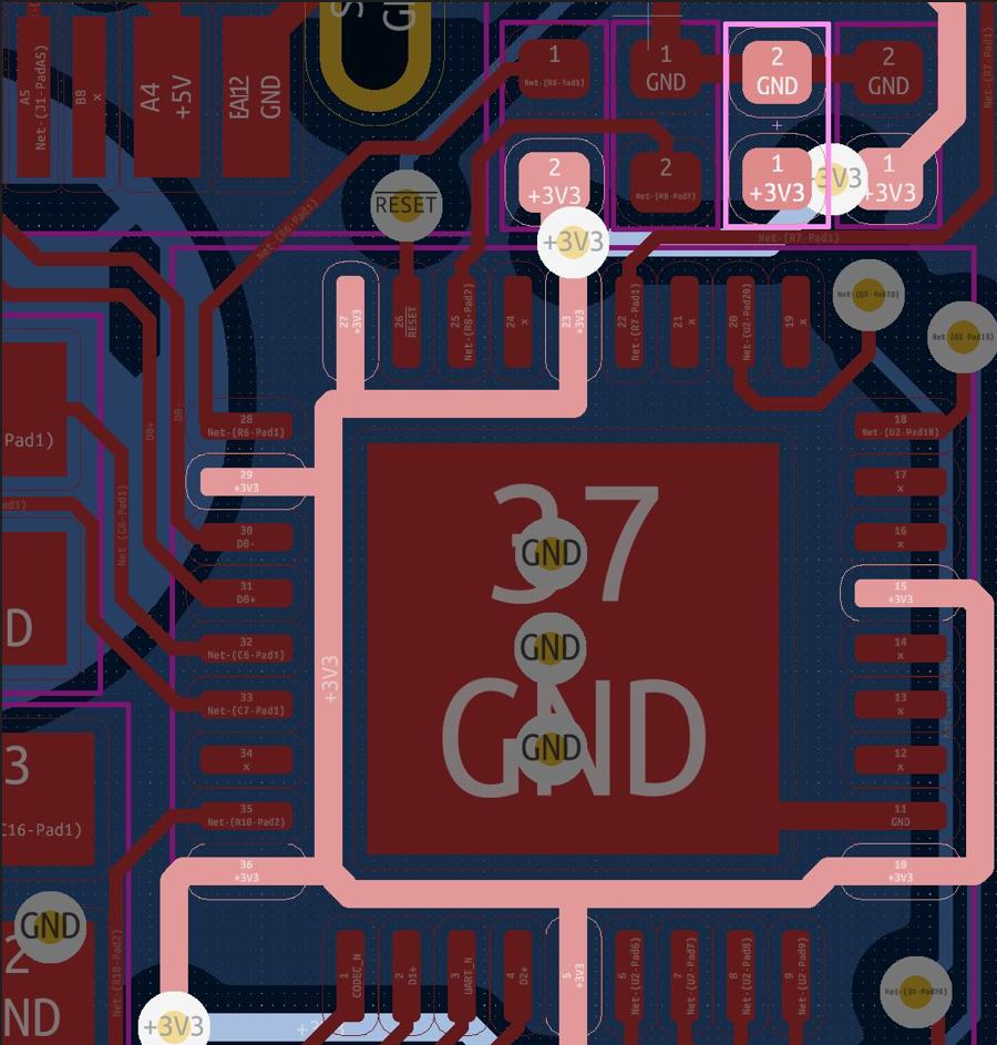
Looks like a nice layout! I guess it will workjust fine in any hobby use case.
If i wanted to "do it the perfect way", i would further improve it by:
- Decoupling each VCC pin with a dedicated 100n on the Top-Side with a similar placement - relative to the pin - as the C on pin 23. I would put a via between the IC pin and the Capacitor (Feel free to use larger pads/smaller drills for these vias to increase copper width around the drillhole, have an eye on production tolerances) connecting VCC to a different layer.
EDIT:
Decoupling capacitors mainly solve a single problem: Source impedance.
Now, a common schematic consits of some application parts and a power supply. On a common board they are seperated by a certain distance and interconnected by tracks and vias and cables and so on.
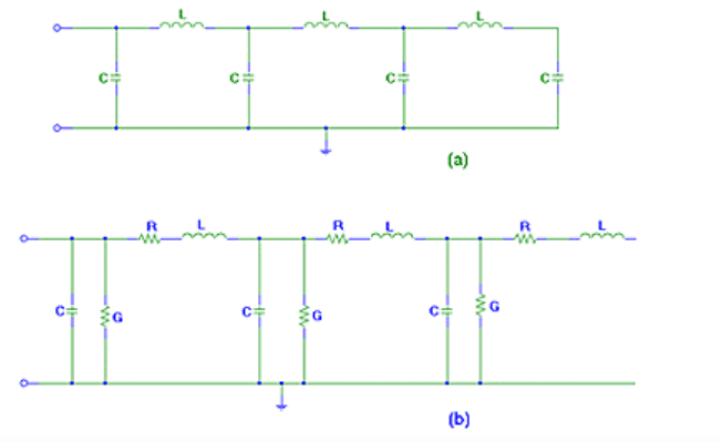
These physical interconnects are not "ideal" components. They can be "imagined" as a series of discrete components. Please see:

Source for PCB Trace Model
This is not a big issue for "pure physical DC circuits". But there are no such circuits. If you are talking about ICs beeing supplied by e.g. 3V3 DC, the source may be an DC-Source. But you logic IC is not a DC-Sink.
It switches, changes state, sets IO-Lines and does a lot of funky stuff- this leads to a change in current consumption - which leads to it beeing an AC-Sink.
So, by now: DC-Source (Model), AC-Sink and complexe interconnects.
Lets say your controller is idle and suddendly requires current to perform some action: This rise in the current consumption needs to be supplied by the source, otherwise the voltage will drop. If the voltage drops too far, the controller will not work reliable anylonger - it can glitch, reset, hang-up, get damaged...tons of scenarios - not of them good.
The ammount of voltage drop for a certain "current request" is dictated by the source impedance - The AC equivalent for DC-Resistance. This impedance is caused by all the inductors and capacitors shown in the "transmission line model".
To avoid a voltage drop, one can place a (in comparison to the parasitic capacitors) huge decoupling cap - typically 100n - close to the IC pin.
The IC requests current, it is supplied from the capacitor with extremly low source impedance - please see ESR: Capacitor ESR and moddeling - and the capacitor is slowly recharged to be ready for the next current consumption spike.
So, by now: Current is supplied continuously to the capacitor from the source. The local and extremly "fast" current consumption spikes are source from the decoupling cap close to the IC. The IC always sees a low source impedance and works fine.
Please see: Document about decoupling caps
The issue now is: If you only use decoupling caps on a single pin and connect this "decoupled" track to other pins, there is a transmission line between the cap and the other pins again. So the effect of the cap is reduced. You can get away with this and on low speed designs it is not that critical.
BUT: The faster the edge-rates (not necessarily the frequency) of your components gets, the more attention you have to pay! A modern SoC will just not work properly. A Avr Mega328p in hobby use...who cares. Now you are working with USB - this puts you somewhere in the middle. Assuming your IC is somewhat recent, it has "fast" edge-rates (Remember edge-rates, not frequency is the main parameter!) even if it is "only" USB 2.0 due to die-shrink and smaller silicone processes.
Please see: Video about decoupling caps in general and Video about measuring bypass caps
Solution: Place a 47n or 100n close to each and every VCC pin. Connect these to your 3V3 rail and doucple this rail (somewhere close to the IC, but not so critical) with 1u/2u2/4u7 whatever. Then provide bulk capacitance (100u or so) at your power supply (Make sure your e.g. LDO can handle such high capacitances!)
Solution: Use a 4-Layer board. They are cheap and available even for hobby use these days. They solve many EMC/SI-related issues caused by bypass problems.
Please see: Video about EMC in generall and Video about PCB optimization
- Removing the trace below the IC ( as it can lead to soldering issues with an exposed pad on the IC caused by soldermask tolerances and so on) and supply VCC via a dedicated plane (4Layer PCB) or a "Half-Moon-Track" connecting all VCC Vias on the Bottom layer and still leaving a sufficient link for the GND-Plane. This plane/half-moon-track would get its own 100u/10u/4u7 decoupling with the 100u close to the power supply and the 10u/4u7 close to the IC.
EDIT:
Your design does most likly match the production capabilitys of your Board-House - that is what Design-Rule-Checks are for.
But, production does always have tolerances - nothing is according to your dimensions specified in your design. Not the track width, nor the solder mask above your track - and especially not the alignement between the soldermask and the copper.
Soldermask and copper are applied in different processes. Between these processes the boards gets moved between machines and so on - misalginement occures.
(1) Routing this track below your IC can lead too - aided by soldermask misalignement and ill-sized copper / solder mask - the track beeing exposed and getting soldered to the bottom of your IC during assembly - now you have a short in your board and it will blow up.
(2) "Your board" is handled carefully by your own - for other persons it is just "a board". It gets scratched during handling, shipping, assembly, inspection and so on. If a scratch in the soldermaks exposes your track copper, and the IC is e.g. misalignet during assembly, a short can occur.
This is why you "never rely on soldermaks as a functional isolator".
(3) Due too production tolerances and a track below the IC, there can be issues with dendrites. On hobby scale you just don't care. As OEM pumping out a million boards a month: You do so very much!
Have a look : Electrochemical migration paper
Please take a deep dive into the topic: Design for manufacturing It is an endless topic with so much to learn! To me it is just amazing!
- Would have a look at "solder wicking" issues with VIAS on a exposed pad. I would solve this issue by this approach: ROHM App Note or the tenting approaches shows in your app note: MicroChip App Note
EDIT:
Now solder wicking from exposed pads is a commonly discussed topic. For hobby use, there won't be any significant problems. But if you want to do automated assembly with high yield, there are some issues with it.
Please see: Impact of Via-In-Pad for QFN and Via-In-Pad from assemblers perspective and Via-In-Pad problems
There is some art, that goes into making a PCB "ready-for-assembly" and providing the best preconditions for high yield and good quality.
Again: Its amazing too me - have a look if you want to learn!
- Would make certain, that no VIAS are close to pads (leave some space between component pad copper and via restring copper) if i did not use VIA-In-Pad production technology - which is expensive. This would prevent yield issues due to stencil misalignment and subsequent solder wicking and/or degassing.
EDIT:
Same issues that can arise from Vias in exposed pads below ICs can also arise when placing vias close-too or in pads of components- They are amplified even, due too smaller solder past ammounts on the smaller components pads.
A rule of thump i always follow is:
(1) If the design is high-density: Spend the extra $ and pay for plugged and capped vias. All problems solved, nothing to worry.
(2) If not high density: Make sure, that vias are always fully (not only the drill hole, but also the entire via copper) coevered with solder mask. Account for tolerances.
(3) If the via is used as test-point (soldermask removed): Make sure, that there is a sufficient "soldermaks-bridge" between the component pad and the via. Account for tolerances.
If you want, you can show images of your entire PCB (Please high resolution).
I am glad to have a look and see, if i can find other opportunitys of change.


