1
\$\begingroup\$

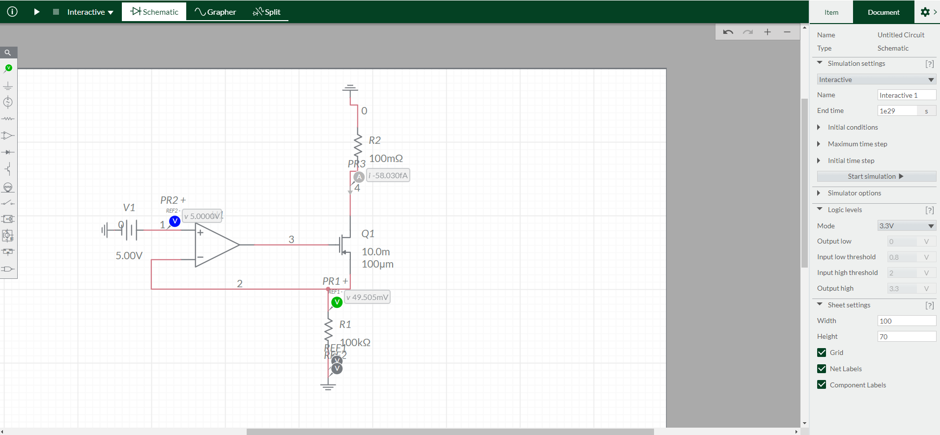
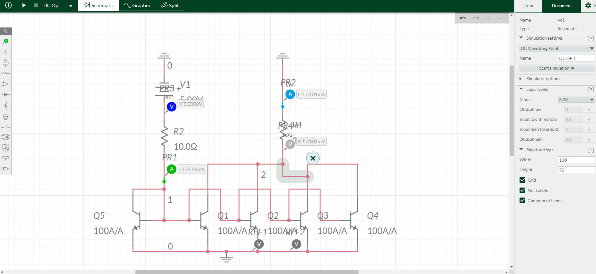
I am getting started on a variable current driving circuit design and just wanted to play around with some of the example circuits I'm reading about, but I never seem to get any meaningful current out - the most I got is 700 mA out of example 2, and that is with a super small load (0.0001 Ω, and the actual load will be 1-10 Ω). I'm hoping to be in the 0.5-5 A range. Can anyone help identify what I am doing wrong?

Example 1:

Example circuit #1

My simulation of example 1

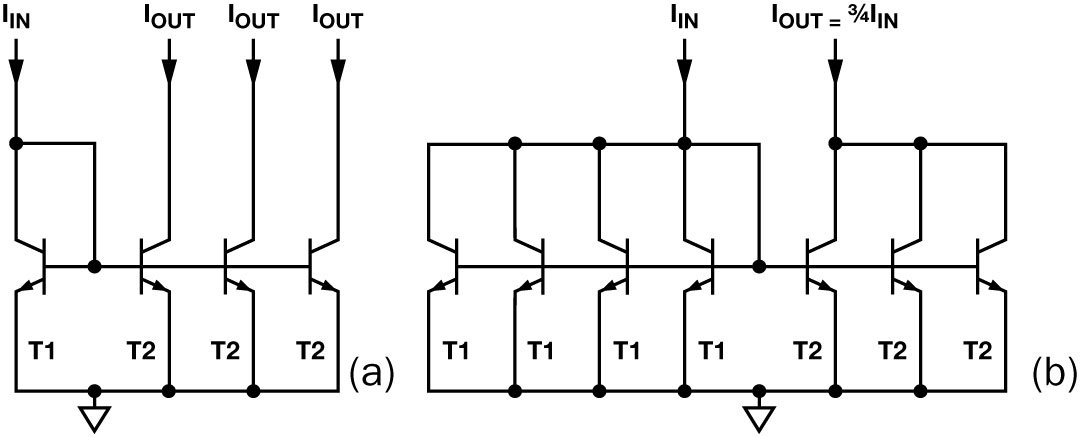
Example 2:

Example circuit #2

My simulation of example 2

Both of my examples are from this article.

\$\endgroup\$
2
  • 2
    \$\begingroup\$ Don't you have both ends of the FET connected to ground in the simulation? \$\endgroup\$
    – JRE
    Commented Mar 13, 2023 at 21:30
  • \$\begingroup\$ @JRE Oh. Yes okay I was thinking about this all wrong. I see that symbol is just a connection - not GND - so adding a voltage source with the bottom node being the positive rail will get me on track? Adding that to the example #2 schematic does give me 2A out now which is certainly closer. \$\endgroup\$
    – InBedded16
    Commented Mar 13, 2023 at 21:37

5 Answers 5

4
\$\begingroup\$

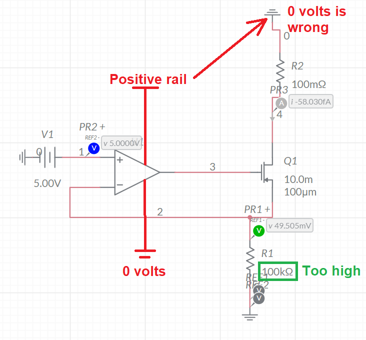
Can anyone help identify what I might be doing wrong?

enter image description here

  • 100 kohm for R1 will get you microamps.
  • R2 needs to connect to a positive supply?
  • MOSFETs don't create current but they can control it providing you have a power source.
  • The op-amp needs a supply (unless using an ideal model)
  • If you want 5 amps out with a 5 volts input, R1 needs to be 1 Ω.
\$\endgroup\$
5
  • \$\begingroup\$ Okay most of this does make sense. The one thing I don't understand is the "0 volts is wrong" part: wouldn't that be applicable for the bottom connection, rather than the top? The one you pointed out is my output current which goes through a resistive load and then to ground. \$\endgroup\$
    – InBedded16
    Commented Mar 13, 2023 at 21:41
  • 1
    \$\begingroup\$ That "wrong" 0 volts needs to be a positive supply and your load has to be R2 in this circuit scenario. If your load must connect to 0 volts then you need a high-side current-controller using a p-channel MOSFET and an appropriate op-amp. What you currently have is a low-side current-controller and the load goes in R2's position (no options) @InBedded16 \$\endgroup\$
    – Andy aka
    Commented Mar 13, 2023 at 22:01
  • 1
    \$\begingroup\$ Note, too, that the available voltage out of the op-amp needs to be sufficient. For a typical "10V" switching FET, that means 5V. Depending on the op-amp, that means a positive supply of between 5V and 10V (and enough to put 12V on the gate is probably safest). \$\endgroup\$
    – TimWescott
    Commented Mar 14, 2023 at 0:24
  • 1
    \$\begingroup\$ @Andyaka ah okay. I was using R2 as a placeholder for my actual load, but I do see how the current flow is opposite of how I was thinking of it. It's just an LED so probably can be low-side or high-side control, but I will go do a much deeper dive on the physics of these circuits before I get into any sort of real design. Thank you for explaining this! \$\endgroup\$
    – InBedded16
    Commented Mar 14, 2023 at 20:10
  • \$\begingroup\$ More options with a low-side driver and, like you said, it doesn't make a difference for an LED. \$\endgroup\$
    – Andy aka
    Commented Mar 14, 2023 at 20:46
1
\$\begingroup\$

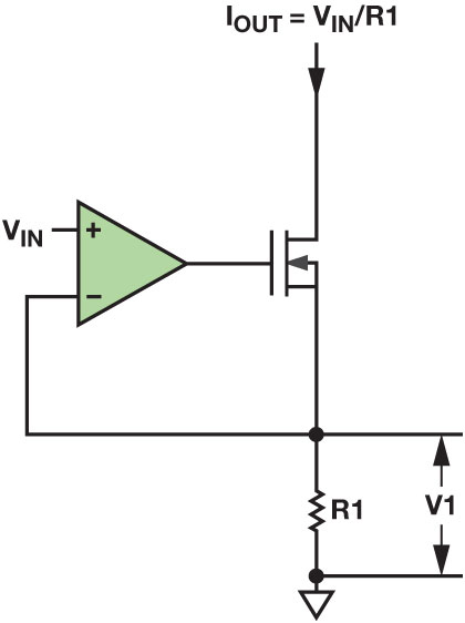
You seem to have gotten an idea that these circuits create current. No, they do not create current, they just limit the current. Something outside the circuit has to try to push the current through the right half, and then, these circuits makes sure the current is the amount you want. For example, the first circuit limits the current to VIN/R1 as the label says.

\$\endgroup\$
1
\$\begingroup\$

These circuits are current sinks -- they don't actively pull current from a source, they can only allow current to flow into them if it would have flowed into ground anyway.

So everywhere that you have a ground connection pointing up, you need to replace that with a suitable voltage source.

Also, for your circuit #2, the author of the article was using chip design rules, where you can count on transistors being well-matched and in intimate contact with one another. For the circuit to work with discrete transistors you need emitter loading resistors on each of your transistors to keep them balanced -- otherwise temperature variations will mess up the current mirror.

There's a tradeoff on how much resistance to use, but enough to drop half a volt at full current probably isn't a bad place to start.

\$\endgroup\$
1
  • 1
    \$\begingroup\$ it's worth noting they are often drawn the same as current sources because an ideal "current source" can either source or sink current depending on what is demanded by the circuit. They draw them as sources and then remember to use them in sink mode. There's no different symbol for a current sink. (Alternatively you could consider that the combination of power supply + current limiter makes a current source) \$\endgroup\$ Commented Mar 15, 2023 at 16:47
1
\$\begingroup\$

In simulations, current sources are able to produce whatever voltage across them needed to have their rated current pass through them. That is, they are energy sources.

Transistors, and op-amps are not energy sources, and the best they can do is borrow energy from someone else, in order to produce some potential difference that will propel the expected current.

This is illustrated here (left), where I use a an artificial current source to obtain 1mA through resistor R1. You will notice that without any help, it's able to produce the exact potential difference across itself, which will in turn apply the necessary voltage across R1 (by KVL), to result in 1mA through the resistor:
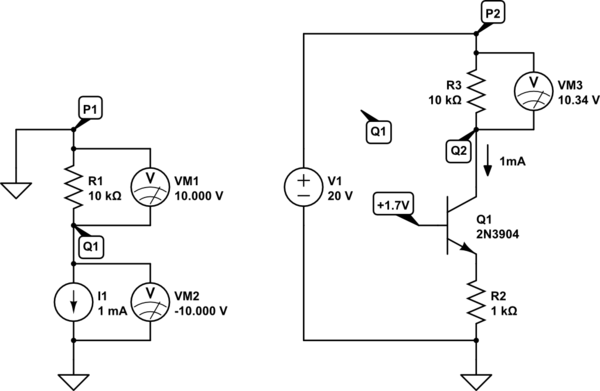
schematic

simulate this circuit – Schematic created using CircuitLab

The important point about the circuit on the left, is that there are no other voltage sources present, and yet I1 is able to provide the necessary potential difference. That's because it's fake, a simulated element, and in simulations we can make any type of component we want. In real life, things are different.

If you are using transistors, op-amps or resistors to build a current source, none of which are able to produce a potential difference on their own, since they are not energy sources, you will need to provide them with a source of energy, whose potential they can use to modulate and regulate current through their load. That's what the circuit on the right is doing.

I use a transistor to set a fixed potential difference across R2 (about 1V here), as you have done in your own designs, but the transistor is not able to magically produce the potential difference across load R3 necessary for 1mA to flow there.

That energy must be provided by a separate voltage source, V1. The potential at Q can't become negative, as it did on the left, because the transistor can't produce any potential difference of it's own. Instead, what we do is make P much more positive, using a separate voltage source, and use the transistor to pass exactly the correct current necessary to "drag" potential Q down to exactly the right amount. The result is the same, 1mA through R3.

In other words, we can use a transistor to pass current produced by another voltage source, but we cannot make the transistor produce a potential difference all on its own. Instead of connecting the top ends of your loads to ground, 0V, there must be a higher potential there (P). Then the transistors can lower the potential at their bottom ends (Q), by becoming conductive, and passing current.

\$\endgroup\$
1
  • \$\begingroup\$ This is a really good explanation. Another answer gave a better breakdown of what I was doing wrong, but this will set me on a good path of how to do it right so thank you. \$\endgroup\$
    – InBedded16
    Commented Mar 14, 2023 at 20:18
0
\$\begingroup\$

For sure like the other answers mention, you need to connect R2 to a high voltage. There is another mistake in your simulation schematic. I think you've wrongly used a PMOS (Q1). It needs to be an NMOS.

\$\endgroup\$

Your Answer

By clicking “Post Your Answer”, you agree to our terms of service and acknowledge you have read our privacy policy.

Not the answer you're looking for? Browse other questions tagged or ask your own question.