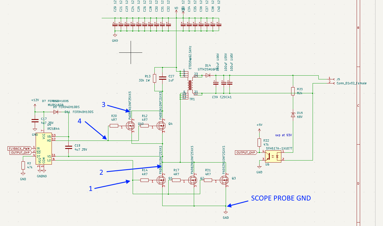
May I make the following comments:
Comment #1:
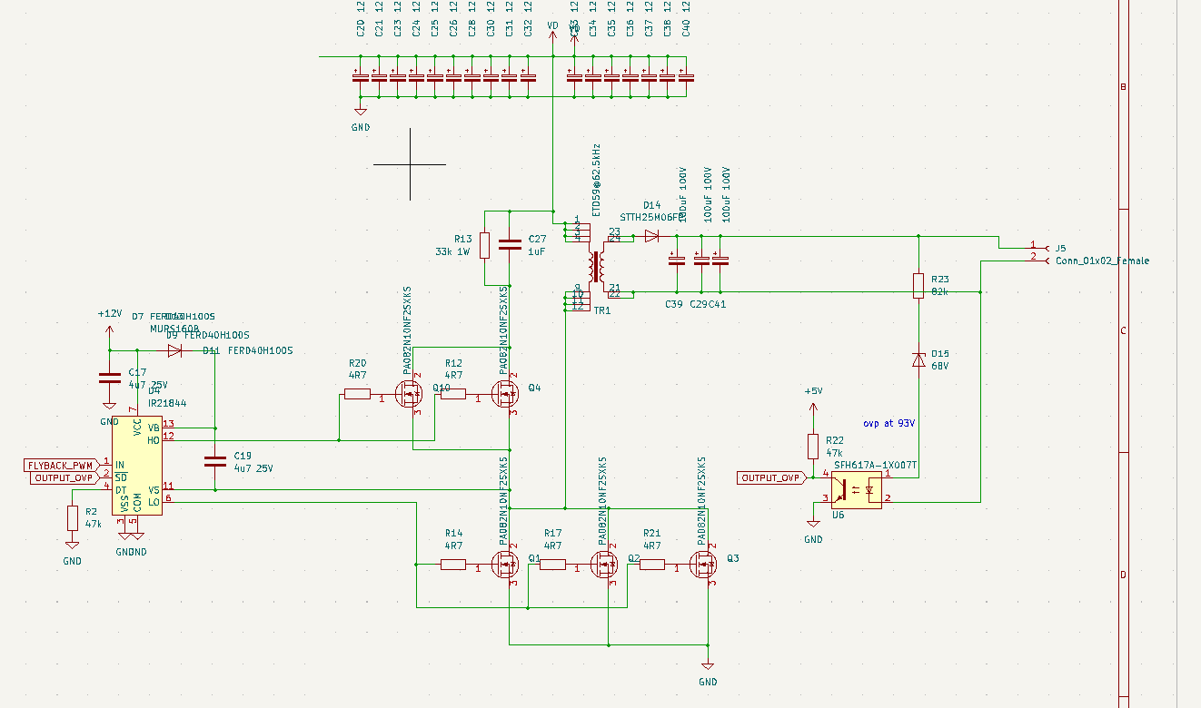
If your scope can display more than one channel, then may I suggest showing as many voltage waveforms as possible simultaneously at the following nodes (refer marked-up diagram below):

Comment #2:
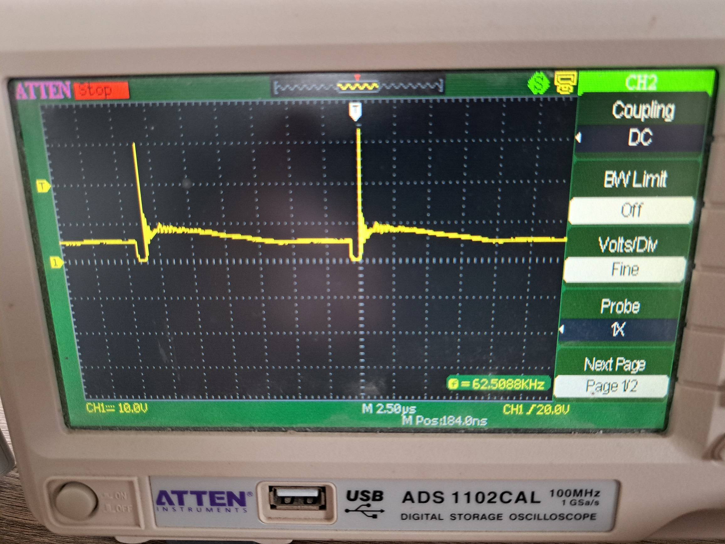
Your concern seems to be: "Is the voltage across Q1 is excessive?"
My reply at this time would be: "Is this problem real?"
The method of probing this circuit will have a big impact on the quality of the waveforms shown on the scope, and will greatly help answer the question: "Is this a real problem or not?"
By "method of probing" what I mean is: "how the voltage signal is transferred from the PCB to the scope input". This includes the probes themselves, as well as the means by which the probe nodes are connected to the circuit node. And by "probe nodes" I mean both the probe tip, and its ground clip. There are many resources on this issue, but I guess as a minimum please apply the following rules.
Glossary: "DUT" = Device Under Test:
Don't use x1 probes. Use x10 or x100.
Don't use switchable probes (x1/x10). If you only have switchable probes, then set them to x10 (or x100), and tape the switch in this position to avoid accidentally changing the switch as you move the probe.
Calibrate all probes before connecting to the DUT.
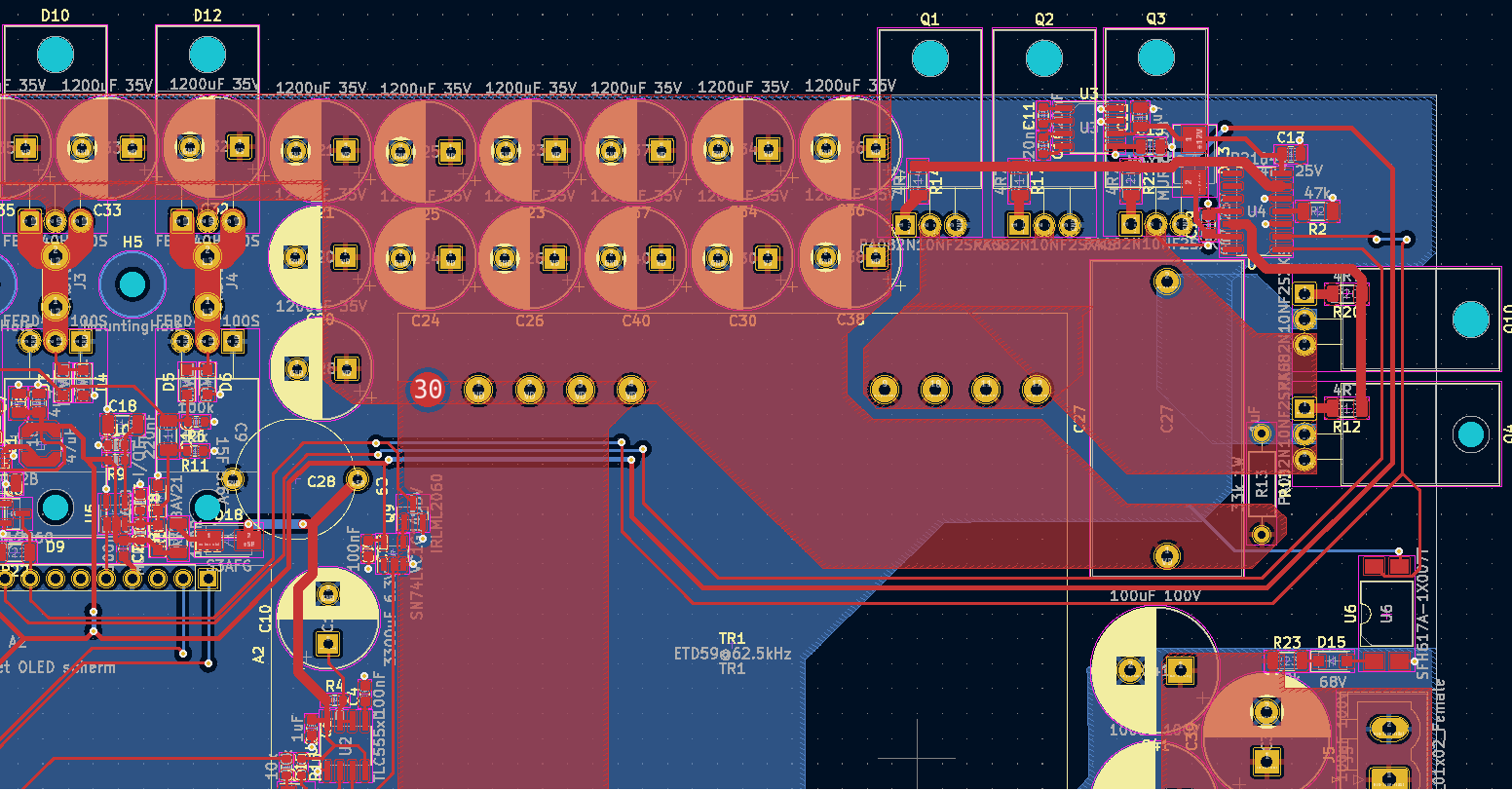
If your probe does not have correct tips for connecting to SMD parts, then temporarily solder one lead of a leaded 1k resistor to the DUT nodes you are probing (1/4W will be more than OK for this). Clip the probe tip to the other lead of the resistor.
Probe GND leads should be as short as possible (less than 100mm).
Connect all probe GND clips to exactly the same point on the DUT. If necessary, solder a temporary stiff wire to the DUT ground plane to make this easier.
To accurately capture very high-frequency signals in a noisy environment (as you have here with this flyback), you may have to use "ground springs", aka "pig-tails" on your probes.
More links to hints about scope probes here:
What do you use to probe small circuits quickly?
What are the differences between a x1 and a x10 osciloscope probe
Does the 1x oscilloscope probe setting slow down MHz digital signals?
How do you attach an oscilloscope ground spring?
Comment #3:
After you have gathered the waveforms accurately without excessive noise, which are presented correctly aligned in time with each other, and then presented with correct voltage scaling & timebase, then it may then be possible to share the results with the community to get help to answer this question:
"Is the problem real?"
If the answer is "yes", then there are many ways to address it, the simplest being putting a suitable voltage clamp in place - however, the best solution will depend on what is uncovered from further investigation. To help the community help you better, then may I suggest including the following information with your next update:
- Good quality waveforms, as discussed above.
- Include these (non-waveform) values at the same time that the waveforms are captured:
(a) Output voltage, current, and power.
(b) Input voltage, current, and power.
(c) From (a) and (b) calculate power loss, and efficiency.
(d) Are any components getting warmer than expected?
Comment #4:
Here are some comments/suggestions that may help make progress towards a solution:
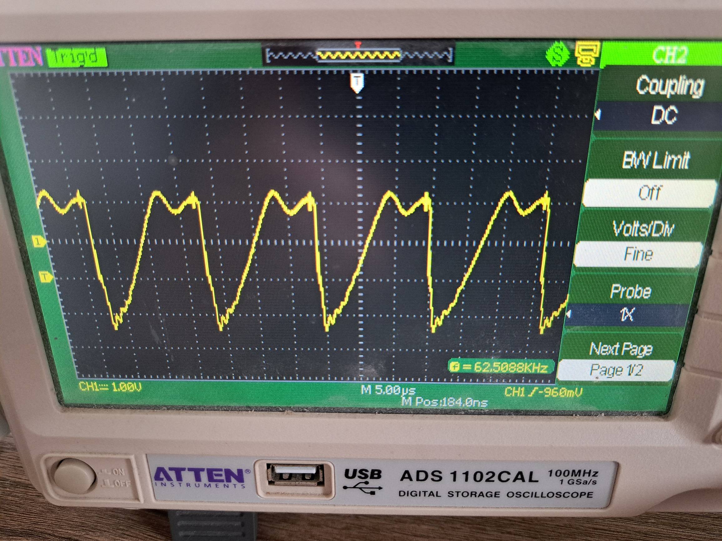
If the circuit is operating as intended, then is the voltage across C27 supposed to be constant, or should it have the ripple that is being shown?
Are the gate drive waveforms as expected? (These are marked as nodes 1 and 4 in the image posted.)
What is the magnetising inductance of TR1 (measured at the primary winding)?
Is the flyback intended to operate in continuous or discontinuous conduction mode?

