2
\$\begingroup\$

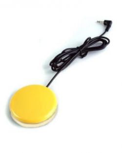
I'm working on a project to add a time delay to the button, so that when pressed, the toy plays for, say, 15 seconds and turns off. The toy is intended for children with disabilities and sometimes they simply lack the strength to hold the button for a long time, and the toy only works when the (monostable) button is pressed.

toy

button

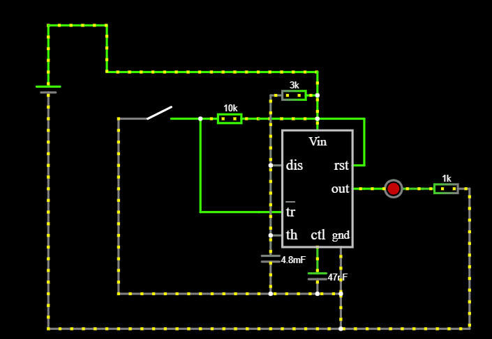
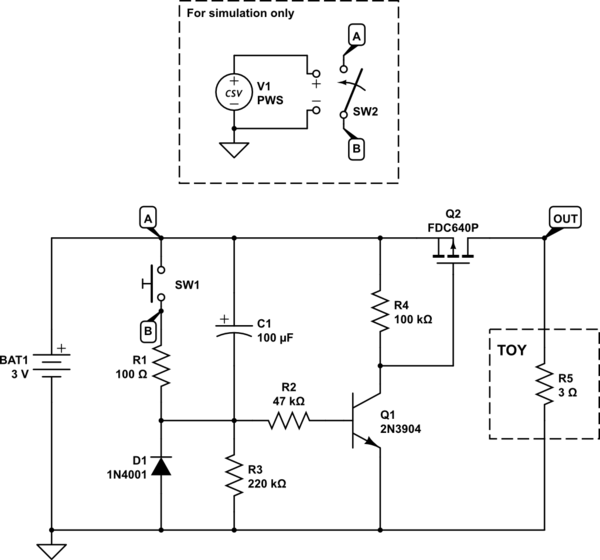
The button is responsible for connecting the power supply, which immediately activates the toy. My idea for adding a delay is to add an encapsulated printed circuit board between the toy and the button. I plan to include a 555 timer circuit on the board and a problem occurred while designing the circuit. Below is the circuit I started with:

circuit

Unfortunately, it will not work as I planned - I will connect OUT to the minus of the battery and this will control the disconnection of the circuit. It will probably be necessary to use an external power supply in this case.

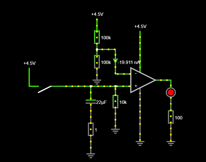
Can someone more experienced give advice on how to improve this solution or whether to use something else? An additional difficulty is that the polarity of the toy powering may be different for different toys (connector are wired randomly because button is polarity independent), so the solution should be insensitive to this. It can use toy voltage or external power supply as well. It would be good if it would be energy efficient. Another idea is to use comparator od CD CMOS timer. Toys are powered with 3V or 4.5V and consumes maximally 1A.

circuit1

\$\endgroup\$
7
  • \$\begingroup\$ Thank you for the update! This is very clear, thanks! Have you measured how much current flows at most when the button is pressed? Also, you say the toy's supply voltage might change. Can we still assume the same polarity (e.g., is the sleeve of the connector always connected to the same side of the toy's internal voltage source)? \$\endgroup\$ Commented Jan 2 at 22:09
  • \$\begingroup\$ Maximal load is 1A when I checked. Unfortunately we can not assume the same polarity. The button is polarity independent and toys doesn't have a standard for polarity. \$\endgroup\$
    – JSK
    Commented Jan 2 at 22:13
  • \$\begingroup\$ If that is the case, then I would have the 555 trigger a small SSR whose load terminals should be able to stand in for the button. \$\endgroup\$
    – vir
    Commented Jan 2 at 22:16
  • \$\begingroup\$ how exactly do you need to have 15s on-time? \$\endgroup\$ Commented Jan 2 at 22:25
  • 1
    \$\begingroup\$ @MichalPodmanický for the NE555, yes. But nobody in their right mind uses these anymore – there's the CMOS variants, e.g. TLC555 \$\endgroup\$ Commented Jan 2 at 23:39

7 Answers 7

2
\$\begingroup\$

So, your 1A current drives up the cost slightly, because you need a slightly larger solid-state relay (SSR).

So, roughly the circuitry would need to contain the following.

  1. A power source. I'd go with a Li-Ion photo cell ("CR123A" or similar, whatever you get cheaply), as these have decades of shelf life, and contain enough charge (typically, 1500 mAh) to power a 30 mA-consuming solid state relay for roughly 50 hours, or 360000× 15s on periods. That should do :) Plus, they're cheap, and easily to source locally.
  2. the connector to the button/switch, and the connector to the toy
  3. A latching MOSFET high-side switch, controlled by the external button
  4. A logic gate (e.g. a simple "NOT"; see a list of viable examples; honestly, go with the SN74LVC1G14DBVR) with a Schmitt trigger input and a supply voltage range covering ca 2.0 V to 3.0 V
  5. a potentiometer through which you charge a capacitor, connected to the Schmitt-triggered input (e.g., a 2 MΩ trimmer, charging a 4.7 µF capacitor)
  6. a solid state relay, controlled by the logic gate (incl. an appropriate series resistor for the input side; assuming you'll use something like the Toshiba TLP241A with 30 mA forward current at 1.27 V typical fwd voltage, you want (3 - 1.27)V / (30 mA) = 56Ω)
  7. you connect the toy to the output side of the SSR

rough sketch of this idea:

sketch

Note that I haven't tested this; you should probably put all this from the left end up to (including) C3 in a simulator. You want low logic-level MOSFETs, so something with a an absolute gate threshold voltage < 1.8 V, i.e. for the p-channel MOSFETs, 0 V > VGS(thresh) > -1.8 V, for the n-channel MOSFETS 0 V < VGS(thresh) < 1.8 V. Candidates are plenty, but an n-Channel option would be the SSM3K16FV, p-Channel SSM3J35AMFV

\$\endgroup\$
8
  • \$\begingroup\$ I simulated the circuit. After each button press it has to be reseted (by pressing button again). Another thing is that the current flows from +BATT to the GND through the R6 even if switched off. For 1k resistor this current is 4mA. The last thing to think about is question about using SSR on the output with 150mΩ resistance. This gives us noticeable voltage drop on the ouput when the current would be 1A. Is it possible to use instead of SSR two mosfets like AO3400 with 48mΩ resistance? N-mosfets with connected gates to the NOT output, sources to the GND and drens to the toy? \$\endgroup\$
    – JSK
    Commented Jan 3 at 16:22
  • \$\begingroup\$ Link to the falstad simulation of the circuit: tinyurl.com/ymuxgzcf \$\endgroup\$
    – JSK
    Commented Jan 3 at 16:23
  • \$\begingroup\$ @Kuba absolutely, you can substitute any other MOSFET. The 150 mΩ one was what I guesstimated to be OK based on length an thickness of cabling, but if it's too much, sure, use a better one! \$\endgroup\$ Commented Jan 3 at 16:59
  • \$\begingroup\$ Thank you for the proposed circuit. It is almost working but there are still the issues which I wrote before, maybe there is something what can be done more \$\endgroup\$
    – JSK
    Commented Jan 3 at 22:27
  • \$\begingroup\$ @Kuba ah so regarding the turn-off: if you used a dual (or more) inverter chip, you could use the output that is currently only controlling the optocoupler, and add another RC "delay" (a few milliseconds) to pull down Q1's gate \$\endgroup\$ Commented Jan 4 at 11:11
1
\$\begingroup\$

Try this:

schematic

simulate this circuit – Schematic created using CircuitLab

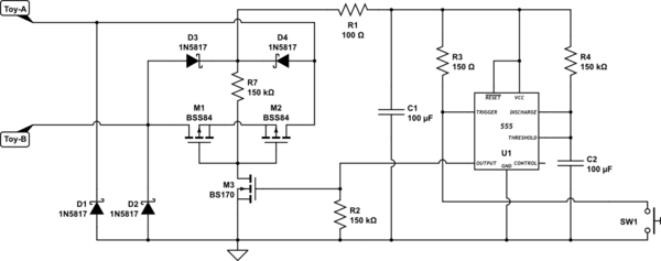
The diodes are arranged as a bridge rectifier to allow the circuit to be polarity-insensitive. Similarly the back-to-back P-FETs form a bidirectional switch.
The diodes you use must be low Vf Schottky type and both the N- and P-FETs must be "logic level" with very low Vgs-th.
You'll also need to make sure you use a CMOS 555 variant which can operate at lower voltages.
When initially connected, C1 charges up through the diode bridge and powers the 555.
The 555 is connected in the standard monostable configuration, so when the button is pressed it'll provide a nominal 16.5 second pulse to the N-FET.
The N-FET then pulls the gates of the P-FETs low to turn them on for the duration to short Toy-A to Toy-B, and during this time the 555 is running off the stored charge in C1.

\$\endgroup\$
0
1
\$\begingroup\$

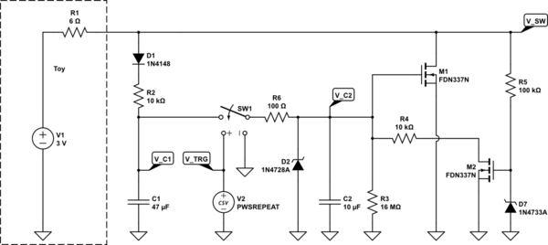
A simple unipolar solution could be this one:

schematic

simulate this circuit – Schematic created using CircuitLab

  • C1 is a precharged energy storage and by closing SW1 a part of the charge is transferred to C2. The value of C1 must be at least 5 times bigger than that of C2 to reach a useful gate voltage at C2.
  • D2 clamps this voltage to produce more or less the same time delay at various input voltages.
  • M1 will turn on and V_SW drops close to 0 V.
  • R3 discharges C2 over time until M1 enters the analog region where V_SW will rise again.
  • To provide a fast turn off M2 was added. It will start conducting if the voltage across M1 (V_SW) is close to 1 V. A FET with an even lower threshold voltage may help here.
  • M2 then discharges C2 via R4 for a quick turn off. Since M2 is initially conducting, it is important, that R4 is big enough to allow the voltage of C2 rising via R6.
  • D7 protects the gate of M2 because FDN337 allows only 8 V here.
  • D1 prohibits the discharge of C1 while M1 is conducting. This allows long closing periods of SW1 and a fast recovery of the function after M1 has turned off.
  • Holding SW1 closed or closing it multiple times in between extends the delay a lot, but I assume this is not a problem in this application.
  • V2 just creates a switch cycle for the simulator run.

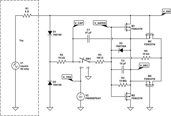
A bipolar version of this circuit would look like this:

schematic

simulate this circuit

  • Either the body diode of M1 or M2 is initially conducting and the switching job is done by the other FET.
  • V_SRC is the negative reference of the timing, a kind of virtual GND, independent of the supply polarity.
  • The supply voltage V1 is implemented as square wave function to show in the simulator, how the circuit works with both polarities.
  • In both circuits the focus was a low voltage drop while the timer is active, because the toy supply voltage can be as low as 3 V.
  • Another topic was a low quiescent current in the inactive state. Only some semiconductor leakage current will flow here.
\$\endgroup\$
5
  • \$\begingroup\$ Thank you for so descriptive answer! I simulated both circuits, the first one works fine and the second one gives me an error "Convergence failed" (in one current direction it's also fine). Is it only a simulation error which I shouldn't worry about? tinyurl.com/28ev67kq \$\endgroup\$
    – JSK
    Commented Feb 24 at 20:13
  • \$\begingroup\$ @JSK The embedded CircuitLab simulator in this site has no problem with this circuit, try it here and look at the time domain simulation. Did you set a GND reference in you simulator? \$\endgroup\$
    – Jens
    Commented Feb 24 at 20:52
  • \$\begingroup\$ @JSK The circuit is perfectly symmetrical, so if it works in one polarity it must work in the other as well. \$\endgroup\$
    – Jens
    Commented Feb 24 at 20:55
  • \$\begingroup\$ OK, thank you! One more question, which resistor could be used as a potentiometer to control the delay? \$\endgroup\$
    – JSK
    Commented Feb 24 at 21:20
  • \$\begingroup\$ @JSK You can split R4 into a potentiometer and a resistor in series. \$\endgroup\$
    – Jens
    Commented Feb 25 at 3:35
1
\$\begingroup\$

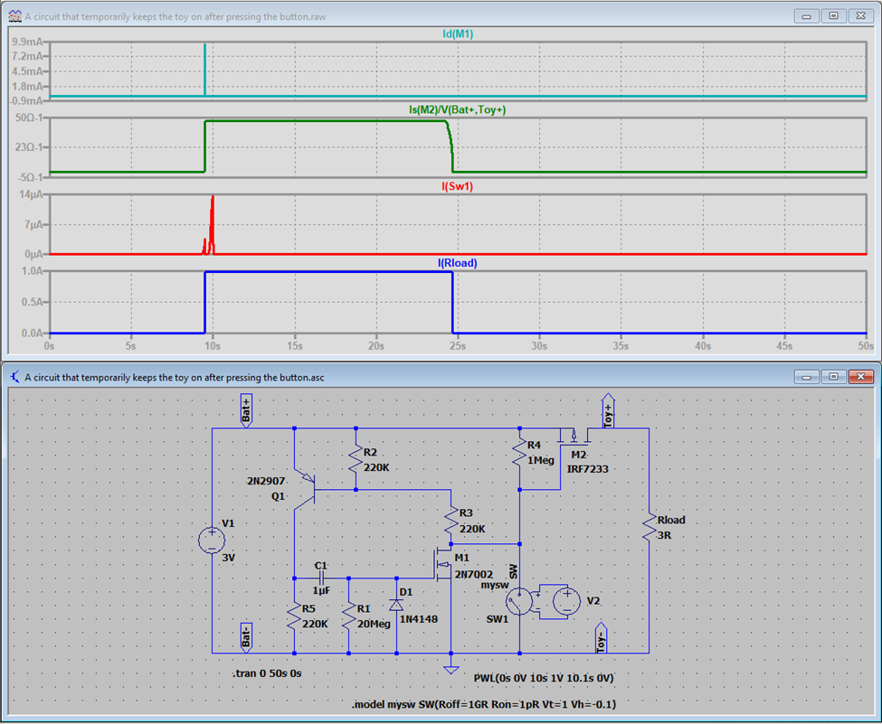
How about the circuit simulated below?

It comes from Figure 3.99D on page 196 of “The Art of Electronics Third Edition” by Paul Horowitz.

The time constant is controlled by R1 and C1, and it will be different for different battery voltages. You can change it by maintaining C1 and changing R1.

You will have to check the transistors (BJT and MOS) that you may have available and their characteristics (mainly the PMOS M2), as this will be the one you want with low RDS(on) so not to drop too much voltage from the battery to the toy.

I have used what the simulator had available. The 2N7002 can be the 2N7000 and Q1 can be any small signal transistor as it does not drain too much current.

I have eliminated the Zener diode because, for a battery of 3V or 4.5V (the original circuit used a 9V battery), I believed it was not necessary.

You can see that it is a compact configuration and you can build it as an extension cable between the battery and the toy.

Thanks.

enter image description here

EDIT:

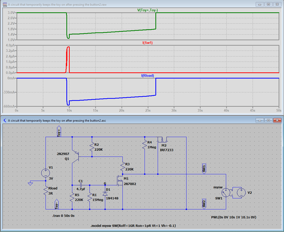
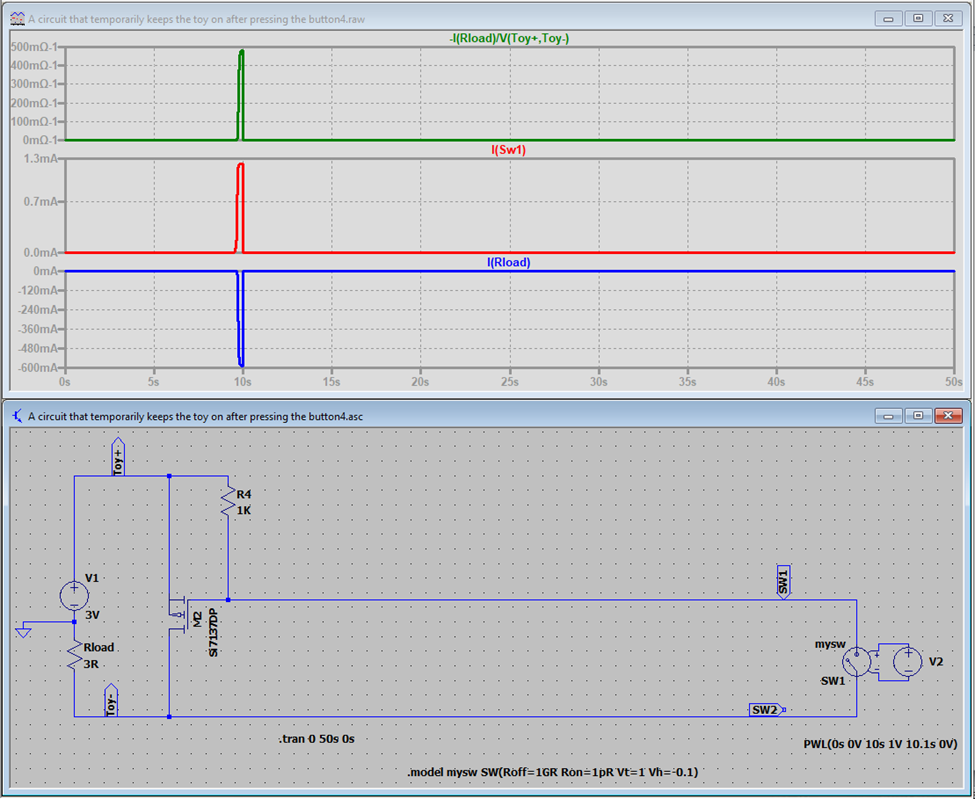
After some thought I realized that my answer does not correctly resolve your problem: The circuit has to be completely separated from the toy and the switch, resting in between them.

So, I have changed my circuit accordingly and have shown the simulation below even though, I know, the polarity of the circuit will still be an issue. To resolve that, you will have to have a connector between the toy and your circuit that can switch its terminals for the correct polarity. I have not considered any other solution for that, as any additional component in the circuit will increase the major problem I am indicating next (look at the Rload current in the chart below).

enter image description here

However, there is a much big problem here. Your circuit will not have the full power of the battery, as the load sits in between them. You just have a fraction of it. Any circuit you install in between them will have the same problem. That is shown in the simulation below where I have eliminated all the components but the PMOS that would drive the load. And that was a PMOS with an RDS(ON) of 2mR. As you can see, when the switch closes, you will only get 60% of the power.

enter image description here

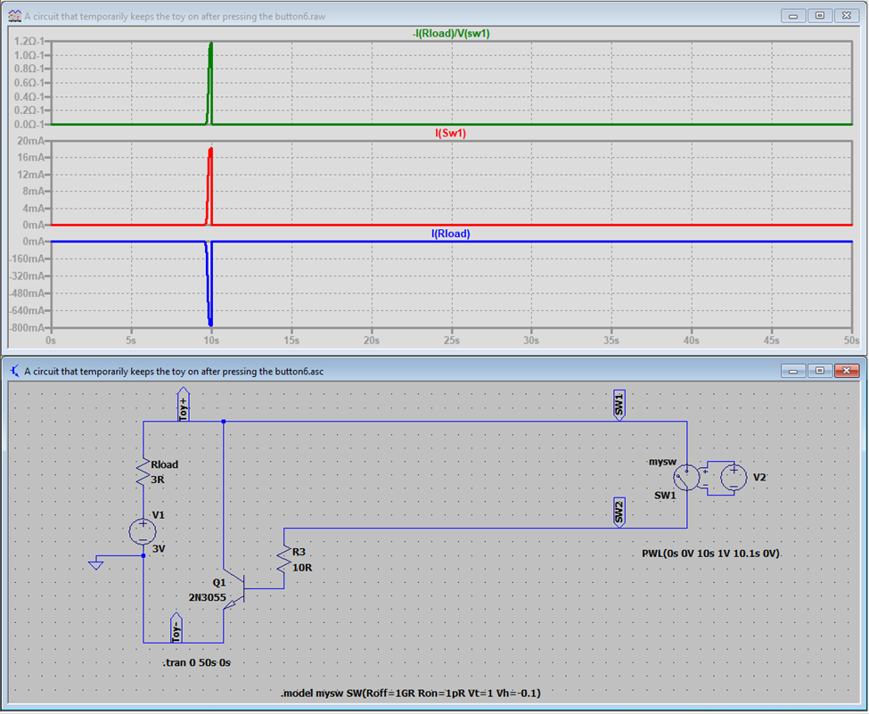
Even if you consider a BJT transistor, which drives more current than the PMOS as it has a lower ON resistance, you still won’t have the full power the toy needs as shown in the simulation below. This is the result of the impedance of the circuit, as shown in the green charts. In the PMOS it was 1/500mR = 2R and the BJT it is 1/1.2R = 0.8333R.

enter image description here

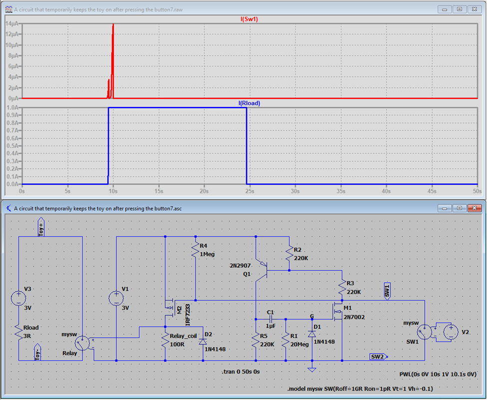
Even an SSR with an RDS(ON) of hundreds of milliohms will not give the toy a full power. Unless you use a RELAY (where the contacts do not depend on the polarity of the connection) and a separated battery (please see the simulation below), any solution will have to be between the battery and the load.

enter image description here

Thanks.

\$\endgroup\$
1
\$\begingroup\$

Here's a two-transistor solution:

schematic

simulate this circuit – Schematic created using CircuitLab

Momentarily pressing SW1 will discharge C1, which will then slowly charge up again. Until the voltage across C1 returns Q1's base to 0.7V, Q1 and Q2 will be on, and the toy is powered.

Using R2 = 47kΩ, and C1 = 100μF, it takes about 15s to return to the off state. You can increase either R2 or C1 to lengthen that delay.

For this to work reliably, Q2 must have \$V_{GS(TH)} < 2V\$, and \$R_{DS(ON)} < 100m\Omega\$.

I nearly forgot to mention, this design draws almost no current from the batteries when the toy is off.

\$\endgroup\$
0
\$\begingroup\$

I believe there is an off the shelf solution for this exact problem https://www.tinyswitchy.com/home

\$\endgroup\$
-1
\$\begingroup\$

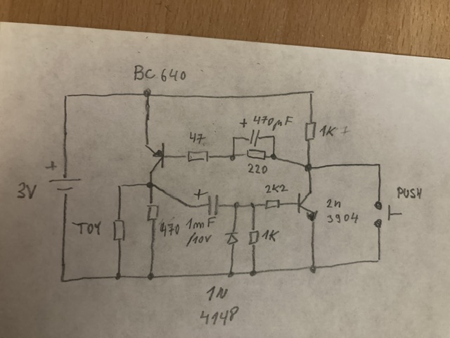
You can try this monostable circuit. The BC640 is 1A transistor , if it is not enough (current or Vce_sat) find one with higher current rating. The 470u cap ensures faster turning off.

The advantage of this circuit is it draws nothing in idle.

enter image description here

\$\endgroup\$
3
  • 1
    \$\begingroup\$ How does this fulfill the job of connecting the contacts of the toy connector? \$\endgroup\$ Commented Jan 3 at 2:16
  • 1
    \$\begingroup\$ Note that op says that polarity of the toy isn't defined, and supply voltage will differ. \$\endgroup\$ Commented Jan 3 at 2:19
  • 1
    \$\begingroup\$ With your circuit, the toy will always be "slightly' on with the 470 ohms in series with its internal power supply. Don't think that works out! \$\endgroup\$ Commented Jan 3 at 2:20

Your Answer

By clicking “Post Your Answer”, you agree to our terms of service and acknowledge you have read our privacy policy.

Not the answer you're looking for? Browse other questions tagged or ask your own question.