1
\$\begingroup\$

I will briefly state my understanding of the following equation, and then pose three questions at the end.
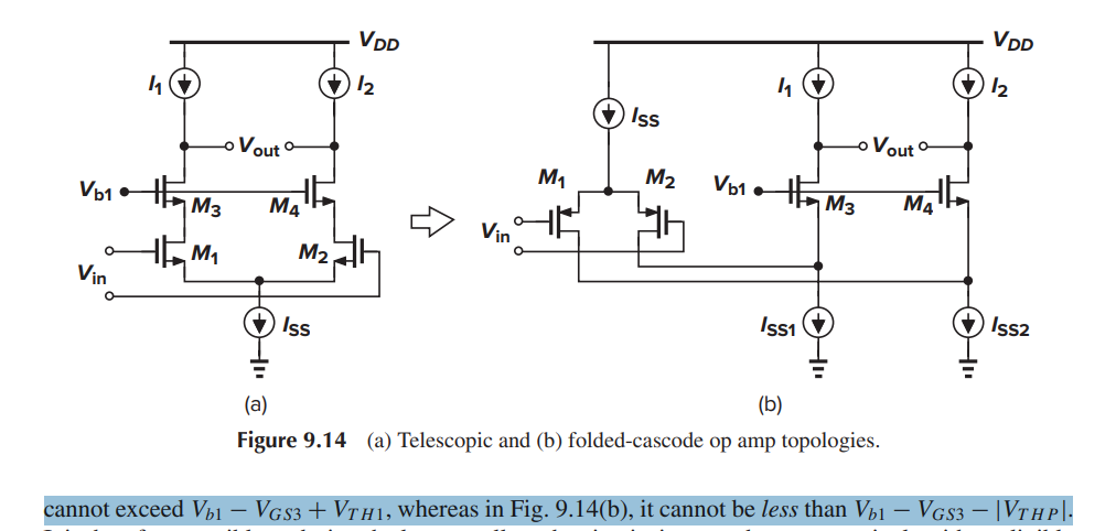
Equation (1) (2) refers to the circuit in the first picture, Equation (3)(4)(5) refers to the circuit in the second picture.

In Razavi’s book, chapter 9.2.4 Folded-cascode op amps, he stated that

In Fig. 9.14(a), the CM input level, cannot exceed
$$V_{b1} − V_{GS3} + V_{TH1} \tag{1}$$ whereas in Fig. 9.14(b), it cannot be less than
$$V_{b1} − V_{GS3} − |V_{THP}| \tag{2}$$ (where \$V_{THP}\$ stands for the threshold voltage of PMOS transistor)

Fig 9.14 Fig.9.14

I am wondering, how is these 2 equations come from?

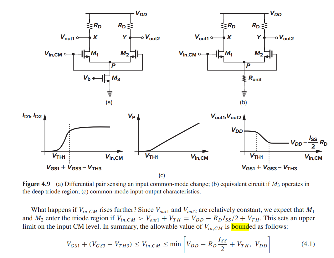
I have searched other parts of the book related to the range of CM input level, trying to find the origin of these two equations. In chapter 4.2, he provides the following formula, as shown in the attached picture.

Fig 4.9 4.9

I think that I understand the right half the inequality equation, that we need to make sure the

\$ V_{DS} \geq V_{OV} \$ so that those transistors not enter into triode region.

But I have confusion about the left half of the inequality equation, for the left half, he stated that

For a sufficiently high \$V_{in,CM}\$ , the drain-source voltage of \$M_3\$ exceeds \$V_{GS3} − V_{TH3}\$, allowing the device to operate in saturation. The total current through \$M_1\$ and \$M_2\$ then remains constant. We conclude that for proper operation, \$V_{in,CM} ≥ V_{GS1} + (V_{GS3} − V_{T H3})\$.

Quote enter image description here

If I understand his words, correctly, his inequality equation.

$$V_{in,CM} - V_{GS1} ≥ + (V_{GS3} − V_{T H3}) \tag{3} $$

Comes from that

$$V_{DS3} ≥ V_{OV3} \tag{4}$$

Then this suggests that

$$V_{in,CM}-V_{GS1}=V_{DS3} \tag{5} $$

I am curious about 3 questions

1: How is the boundary of CM input level of folded cascode amplifier calculated, that is to say, how is equation (1) and equation (2) derived from?

2: Is there any relation between the inequality of Fig 9.14 and Fig 4.9?

3: How is the Drain source voltage of transistor 3 in Fig 4.9 equal to \$ V_{in,CM}-V_{GS1} \$, that is, how is equation 5 derived from?

\$\endgroup\$
6
  • 1
    \$\begingroup\$ When it says \$V_{GS3}\$ does it mean \$V_{GS(M3)}\$? It seems your question is about two different circuits so, maybe, it might be better to concentrate on one. \$\endgroup\$
    – Andy aka
    Commented Feb 24 at 13:09
  • 1
    \$\begingroup\$ Eq1 and Eq2 are both saying that, the input differential pair needs to be working in saturation region. Vb1-Vgs3 is simply the voltage at the drain of the transistor in both case, and for a transistor to work in saturation - Vds > Vgs - Vth. \$\endgroup\$
    – Jack Black
    Commented Feb 24 at 13:33
  • \$\begingroup\$ @GeogreGuo Why Vb1-Vgs3 is equal to the drain voltage of the transistor, I think I just forgot this part of knowledge, may you give me a reference? \$\endgroup\$
    – Tong Su
    Commented Feb 24 at 14:21
  • \$\begingroup\$ @GeorgeGuo, I understand that Eq1 is saying the transistor need to work at saturation region, bu How is Eq2 also implies this? Eq.2 is saying that Vin,cm “cannont be less than” \$V_{b1} − V_{GS3} − |V_{THP}| \tag{2}\$ That is , $$V_{in,CM} \geq V_{b1} − V_{GS3} − |V_{THP}|$$ . To satisfy the saturation condition$$ Vds> Vgs- Vth $$ If $$ V_{b1} − V_{GS3} \ = V_{DS1}$$ suggests to the drain source voltage of transistor \$M_1\$ in Figure 9.14 \$\endgroup\$
    – Tong Su
    Commented Feb 24 at 14:22
  • 2
    \$\begingroup\$ Hi @TongSu. Sorry I wasn't clear. The difference for PMOS FETs is that, the saturation condition becomes Vsd > Vsg - |VthP|. For example, Vsd is now Vs - (Vb1-Vgs). The minus sign in front of (Vb1-Vgs) is the reason for "cannot be less than". Maybe have a look at the answer below, he has done a much better job explaining this. \$\endgroup\$
    – Jack Black
    Commented Feb 24 at 17:15

1 Answer 1

1
\$\begingroup\$

About fig. 9.14 a) & b).

a) $$ V_{g_1}-V_{s_1} - V_{th_1} \leq V_{d_1}-V_{s_1} $$

Simplify: $$ V_{g_1}-V_{th_1} \leq V_{d_1} $$ Mind you, \$V_{g_1}=V_{g_2}=V_{cm}\$ (same for picture b).

Then, we can write the drain voltage of M1 as: $$ V_{d_1} = V_{s_3} = V_{b_1} - V_{gs_3} $$ In other words, we "walk" down from \$V_{b_1}\$ by a \$V_{gs}\$ term.

Then, replace \$V_{d_1}\$ by the last expression: $$ V_{g_1}-V_{th_1} \leq V_{b_1}-V_{gs_3} $$ Re-arranging: $$ V_{g_1} \leq V_{b_1}-V_{gs_3} +V_{th_1} $$ Done.


Start the same way for picture b). I'll skip the 1st step (I started from the \$V_{sg}\$ because it's a PMOS.) : $$ -V_{g_1} - |V_{th_1}| \leq -V_{d_1} $$ We know that \$V_{d_1} = V_{b_1} - V_{gs_3}\$ here as well. First, get rid of the minus signs and isolate \$V_{g_1}\$: $$ V_{g_1} \geq V_{d_1} - |V_{th_1}| $$

Replace the \$V_{d_1}\$ term with its equivalent as we did picture a) and we're done: $$ V_{g_1} \geq V_{b_1} - V_{gs_3} - |V_{th_1}| $$

Razavi wrote \$V_{thp}\$, but that's to probably notate it's a PMOS, he's definitely referring to M1 in picture b.


On to your Question 2).

I believe, since he's using an actual transistor to implement the tail current of those diff. amps in picture 4.9 (unlike picture 9.14), then he can also write both top and bottom limits of the common-mode voltage at the input; you cannot go too high because M1 will be out of saturation, and you cannot go too low because M3 will stop behaving like a current source.

He probably didn't use the other limit in picture 9.14 because an ideal current source has no minimum compliance voltage at it's terminals; they can be negative and the current will still be flowing, it's ideal after all.

Question 3)

It's easy to see that going from \$V_{cm,in}\$ down to the drain of M3 requires us to drop by a \$V_{gs}\$ term, which is the drop across gate-to-source voltage of M1.

\$\endgroup\$

Your Answer

By clicking “Post Your Answer”, you agree to our terms of service and acknowledge you have read our privacy policy.

Not the answer you're looking for? Browse other questions tagged or ask your own question.