5
\$\begingroup\$

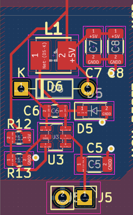
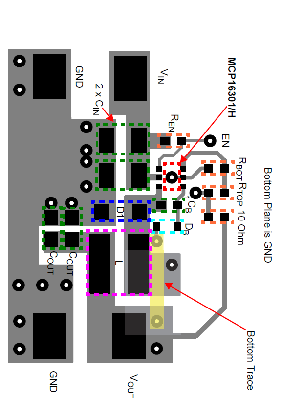
Looking through recommended PCB designs for buck converters, I have noticed that their 'traces' are not usually direct lines, but rather polygons connecting each component.

What is the advantage of using polygonal copper pours(1) over straight traces(2)?

First image is taken from the MCP16301 datasheet, second image is the same design, however routed with regular traces rather than polygonal pours, and only using 1 input capacitor with no EN resistor. The second image is also configured for a 5V output rather than a 3.3V, this has little difference apart from different component values. Input is from connector J5, output voltage is the trace at the very top of the image. A global GND layer covers the entirety of the bottom layer.

enter image description here enter image description here

\$\endgroup\$
1

3 Answers 3

4
\$\begingroup\$

As the two other answers said, more copper equals lower resistance and lower inductance, which measures for high \$\frac{\mathrm{d}\,I}{\mathrm{d}t}\$ things like switching currents through an inductor in a buck converter.

Don't overdo it, though: While not using the thin signal traces you'd use for low currents elsewhere on the board definitely is a good idea, at some point most current will already run on the edges of your trace, and adding more volume just won't help as much. Going wild on PCB copper area won't help immensely much if the bulk of your parasitic effects come from something else!

And: it's probably more important that you improve grounding of U3 than it is to maximize trace width everywhere. Would I review your circuit, I would indeed say "use wider traces", but I'd be more concerned with you trying to carry all U3's ground current through the small via that you use for your feedback voltage divider. That seems like a bad idea; the datasheet's design advice especially tells you to keep the ground path short, between decoupling caps and GND path. You kind of did the opposite: you placed the ground via of the decoupling capacitor as far away from your chip's ground pad as possible without explicitly adding a long trace, and you also routed your device ground on the top layer for a while, further away from both the ground pin and the desirable location of the decoupling capacitor. Simply use two separate vias for your U3 ground pin and the ground of your voltage divider, and flip your C5 around, so that its ground via is closer to the chip.

\$\endgroup\$
2
  • \$\begingroup\$ nitpick: for switching currents in a dcdc coil it's not the lower inductance that's important, but rather lower capacitance. \$\endgroup\$ Commented Apr 3 at 14:50
  • \$\begingroup\$ @VladimirCravero true, but you don't get that with wider traces \$\endgroup\$ Commented Apr 3 at 15:13
8
\$\begingroup\$

What is the advantage of using polygonal copper pours(1) over straight traces(2)?

Lower inductance and resistance at no added cost since you’re paying for the whole PCB anyway.

Try to move to smaller capsules (are you using 0805?), change the THT diode to SMD, tighten up the switching loop as much as possible and use polygon pours wherever you can.

\$\endgroup\$
8
  • 2
    \$\begingroup\$ And better heat removal. \$\endgroup\$
    – MOSFET
    Commented Apr 2 at 14:30
  • \$\begingroup\$ Yes, most of my resistors and capacitors are 0805. What do you mean by 'switching loop', and would significantly thicker traces(1mm vs 0.3mm I used earlier) work? \$\endgroup\$
    – lemon
    Commented Apr 2 at 23:49
  • 2
    \$\begingroup\$ @lemon By switching loop, it means the closed path from the switching node, to output capacitor, to capacitor ground, and to converter's ground pin. It's important to realize that inductance is not a property of "inductors", instead, it comes from the magnetic field around closed loops. Thus, (1) all closed loops have inductance. Furthermore, the inductance of a circuit is (2) positively correlated to the enclosed loop area. Thus, to minimize parasitic inductance, the power and ground must be very close to each other, and the best way is to use solid copper pours and ground planes. \$\endgroup\$ Commented Apr 3 at 4:18
  • \$\begingroup\$ Move down to 0603 or 0402 if you can. Thicker traces help, but why are you reluctant to use polygons? \$\endgroup\$
    – winny
    Commented Apr 3 at 6:01
  • 1
    \$\begingroup\$ I'm far from a regulator layout person, but how to tell the EDA tool where to connect the regulator ground to the common ground in a sensible way seems to be a very common, recurring problem. I've seen all manner of dirty hacks to solve this, like zero ohm resistors and the like. \$\endgroup\$
    – Lundin
    Commented Apr 3 at 13:39
5
\$\begingroup\$

The difference is the same as connecting anything with small long wires or big short wires.

High frequency current pulses do no pass well through wire inductance, high currents cause higher voltage drop on thin wiring.

Any current running around in a loop is an antenna that radiates energy so large loops radiate more current.

Those are the reasons to keep wiring between components wide and short while minimizing loop area.

For example you take the 5V output directly from inductor, but there is another wire branch to the output capacitor. So the output has more ripple as the capacitor cannot affect it as it has a separate narrow wire with inductance and resistance to inductor output.

\$\endgroup\$

Your Answer

By clicking “Post Your Answer”, you agree to our terms of service and acknowledge you have read our privacy policy.

Not the answer you're looking for? Browse other questions tagged or ask your own question.