6
\$\begingroup\$

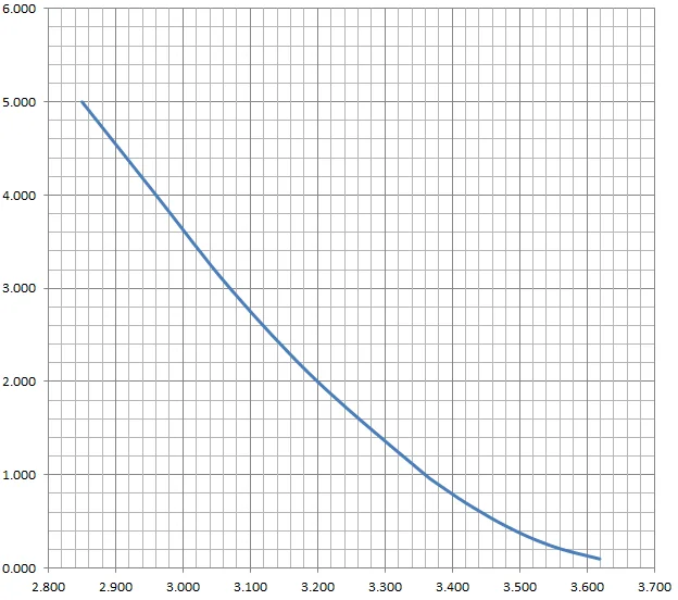
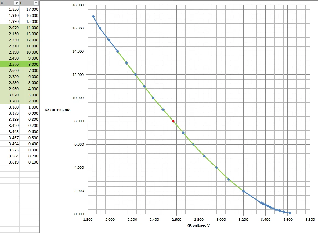
I have a bunch of J112 JFETs and would like to use them for high impedance input stage, but I'm a bit confused because the datasheet says that its Idss should be about 5 mA, but when I measured it, I already get 17 mA at -1.85 V at the gate (with 12 V supply voltage), it started to dissipate quite a lot of power, so I stopped increasing the gate voltage. Is it normal for it to behave like that?

I found what looks like a nice linear region (painted it green, gate voltages are negative of course, just used absolute values for the chart) in the characteristic with bias point set to -2.570 V and 8 mA, can I use my JFET in this region? If the current exceeds Idss, won't it damage the device (given I don't exceed the maximum power dissipation), or should I still use the region below 5 mA? It's kinda curved down there (the second graph) and bias voltage seems too low at <-3 V.

enter image description here

enter image description here

\$\endgroup\$
3
  • \$\begingroup\$ Where in datasheet it say that Idss should be around 5 mA? Datasheet only give you minimum Idss and Idss spread is usually very large (300%) even for those JFETs that also provide typical and maximum values. \$\endgroup\$
    – Rokta
    Commented Aug 29 at 12:57
  • 2
    \$\begingroup\$ The datasheet only guarantees Idss to be at least 5mA. The actually value can be anything above that and will probably show quite some variation between the individual JFETs. To limit transistor dissipation, pulse testing with very low duty cycle is used to measure Idss. Go down with your DS voltage (5... 6V) while measuring Idss to stay below the rated 0.625W. \$\endgroup\$
    – Raonoke
    Commented Aug 29 at 13:08
  • 1
    \$\begingroup\$ FWIW, checking a couple SPICE models for the J112, the typical simulated Idss with 12V is 38mA (Philips) or 27mA (Linear Systems). \$\endgroup\$ Commented Aug 29 at 14:24

2 Answers 2

7
\$\begingroup\$

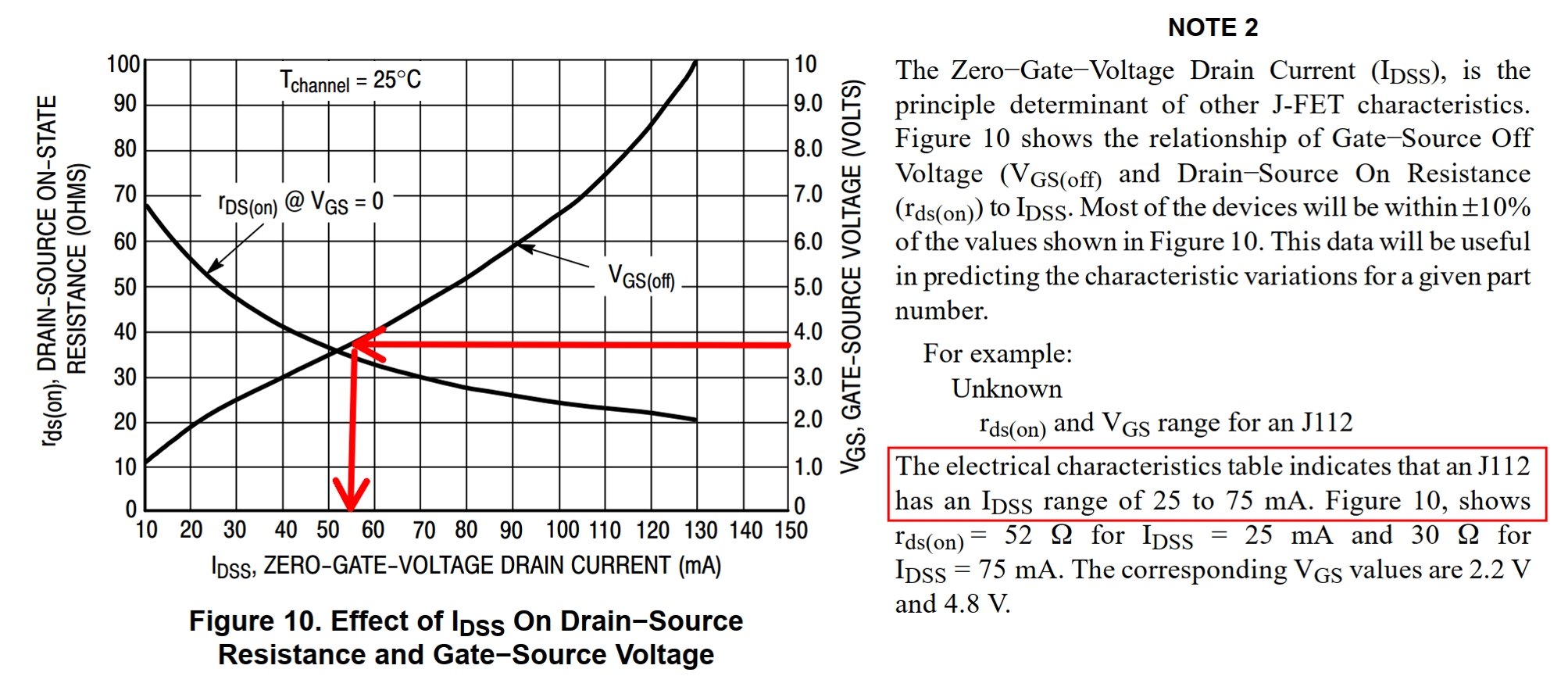
The Idss current of JFETs varies greatly between different pieces. Based on the graph on page four of the datasheet cited, the Idss current of your example is should be around 55 mA. In other words, you measured good values, the JFET is usable, you just have to watch out for maximum dissipation. j112 jfet

\$\endgroup\$
4
  • \$\begingroup\$ What did this figure come from? -- A citation is required. \$\endgroup\$ Commented Aug 29 at 16:15
  • \$\begingroup\$ From the datasheet. \$\endgroup\$
    – csabahu
    Commented Aug 29 at 20:03
  • \$\begingroup\$ See: electronics.stackexchange.com/help/referencing Linking in comments is not adequate as comments can be removed; editing the link into the post, with mention of where (e.g. figure, page number) the copied material came from, gives a clear and precise indication of what has been quoted. \$\endgroup\$ Commented Aug 29 at 20:10
  • 1
    \$\begingroup\$ Thanks, I have modified it. \$\endgroup\$
    – csabahu
    Commented Aug 29 at 20:15
5
\$\begingroup\$

J112 specifies a minimum of 5mA, and no maximum, IDSS. Your parts are not constrained by this parameter.

RDS(on) likewise only sets a maximum.

They will however be constrained in terms of capacitance: large IDSS due to a too-large junction would have excessive C. This can be measured with a sensitive capacitor meter, possibly with some means to apply bias (to ensure the G-channel junction is reverse biased).

You may want to check gate cutoff voltage as well. (The plot suggests something around -4V, which is as specified.)

As for suitability, we cannot assess that without knowing what circuit it is to be placed in, or what function the circuit is supposed to perform.

\$\endgroup\$

Your Answer

By clicking “Post Your Answer”, you agree to our terms of service and acknowledge you have read our privacy policy.

Not the answer you're looking for? Browse other questions tagged or ask your own question.