0
\$\begingroup\$

I was asked to calculate the voltage gain of a circuit containing 2 P-MOS and one N-MOS transistors: enter image description here
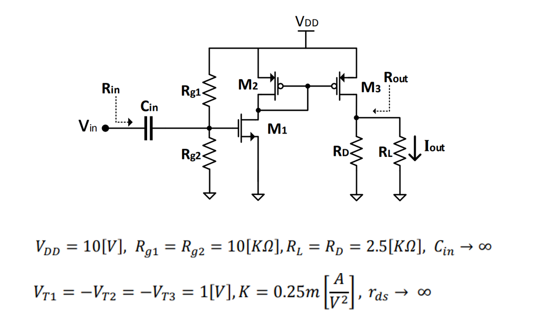
I calculated the operating point and got: gm1 = gm2 = gm3 = 2 [ms] The circuit that I built for small signal analysis was: enter image description here

but now I am not sure how to find the relationship between Vin and Vout.

EDIT: Ignore the Rds resistor, it is for another question.

\$\endgroup\$
1
  • \$\begingroup\$ Raed Jayyousi - Hi, Where did that image come from? To comply with the site rule on referencing, details of the original source of copied / adapted material must be provided by you, next to each copied / adapted item. If the original source is online & public, please edit the question & add the webpage/PDF name & its link (URL) (e.g. website name + webpage title + its URL). If the source is offline (e.g. book or private intranet) then edit the question & add full source details e.g. title, author, page, publisher, edition. TY (More site rules in the tour & help center.) \$\endgroup\$
    – SamGibson
    Commented Sep 14 at 16:14

2 Answers 2

0
\$\begingroup\$

See M2 & M3 form a current mirror -- M3's current is equal to M2. M2's current is equal to M1.

For your (homework ?) answer, be sure to include the polarity (+ or -) of the gain.

\$\endgroup\$
0
\$\begingroup\$

There are two inverting stages. Ignoring rds, the gain of each stage is determined by gm times drain load. The load in the 1st stage is a diode connected PMOS. First stage gain is Av1 = - gm1 * 1/gm2 and 2nd stage gain is Av2 = - gm3 * (RD || RL). Total gain would then be Av = Av1 * Av2. With gm1 = gm2 = gm3 = gm the overall gain is Av = gm * (RD || RL).

\$\endgroup\$

Your Answer

By clicking “Post Your Answer”, you agree to our terms of service and acknowledge you have read our privacy policy.

Not the answer you're looking for? Browse other questions tagged or ask your own question.