2
\$\begingroup\$

I'm trying to develop a circuit that can generate a pulse signal that meets the following requirements.

  • The power supply is 3V.
  • The output voltage of the signal must be adjustable from 12 to 60V.
  • The pulse width must be adjustable from 100 µs to maximum 500 µs.
  • The frequency must be adjustable from 1Hz to 1000Hz.
  • Since the voltage is boosted so much, the current may be very small.

My first idea was to split the problem in two different problems:

  1. A way to boost the supplied 3V to a steady 60V and use that voltage as "input".
  2. The easier part: switch the 12-60V with a MOSFET that is controlled by a microcontroller.

The second subproblem is very easy. I used an ESP32 to switch a MOSFET in the desired frequency and pulse length. The microcontroller is fast enough to time the signal accurately. I wrote simple code and measured the resulting signal with an oscilloscope, and it works.

For the first problem: My thinking was that when I find a way to boost 3V to 60V (or voltages inbetween since this must be adjustable), I can simply use that voltage to do with it whatever I want. I imagine this created voltage as the new "input" voltage for subproblem 2 (the switching).

But I've not seen a boost circuit that can boost the voltage so much to get 60V from 3V.

I think the solution is more complex. I should probably use the discharge voltage of an inductor directly and use that voltage spikes as the pulses. The inductor "switching" can be done at the desired signal frequency (1 - 1000Hz). Then, every signal pulse is just a discharge spike from the inductor that unloads. When approaching it this way, the question is how to manipulate that inductor's discharge pulse to meet the requirements of pulse width and voltage.

Does someone have an example or name of a circuit that works this way, or maybe a totally different solution?

\$\endgroup\$
6
  • \$\begingroup\$ What is the load? How is the voltage adjusted? What is the tolerance on the voltage level? \$\endgroup\$
    – Mattman944
    Commented Nov 24 at 22:58
  • \$\begingroup\$ Load is around 10k to 15kΩ. Voltage is adjusted by controlling the switching frequency in a boost converter (if boost converter approach is used), and voltage tolerance is 5%, but I'm happy if we get close. \$\endgroup\$ Commented Nov 24 at 23:39
  • \$\begingroup\$ Boosting to 60V is easy under 1/2W. Is the load floating or do you need a common ground with a hi-side switch. Lo-side is simpler. \$\endgroup\$
    – D.A.S.
    Commented Nov 25 at 1:09
  • \$\begingroup\$ What I meant was: how is the voltage set? Pot? Some type of MCU input? \$\endgroup\$
    – Mattman944
    Commented Nov 25 at 2:24
  • \$\begingroup\$ Does the pulses need to be pure square? Or can they be rounded by capacitor? \$\endgroup\$ Commented Nov 25 at 10:58

5 Answers 5

3
\$\begingroup\$

Use a coupled inductor flyback boost topology, where the flyback inductor has two windings (or a single tapped winding) so it gets both a transformer step-up and a flyback kick.

maybe start with the flyback transformer from a phone charger, or the 5VSB circuit in a pc power-supply.

\$\endgroup\$
3
\$\begingroup\$

To get 60V from 3V is not difficult, but not trivial either. You should probably ask another question on the site dedicated to that task alone, but be specific about your requirements. Nobody here knows what you mean when you say "very small current". As already suggested, cascading two boost converters would be one way to go. Also, be aware that if you require a precisely regulated pulse height, then you'll need more than 60V, maybe 65V would be a better target.

From here on, I assume you already have a source of +65V DC.

It is not clear whether you wish the output to be a "short-lived connection" to +60V (or whatever voltage you set) as a momentary switch would do, or an output that both pushes potential up to +60V and then actively pulls it quickly back down to zero, a so called push-pull output. The two are very different, the latter being significantly more complex.

I will assume the the former.

You do not mention the load at all, and we are left to guess what kind of thing you are connecting to this output. If the load is at all inductive or capacitive, then the circuit instantly doubles in difficulty, and there's a good chance what I suggest here will be useless to you.

I will assume a purely resistive load, drawing no more than 50mA.

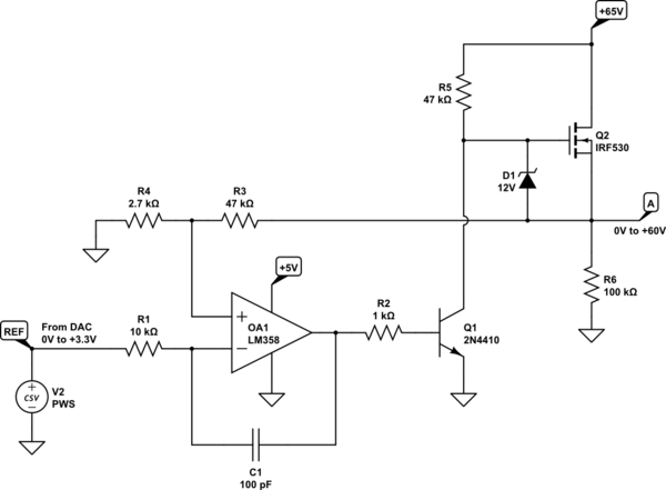
Your ESP32 has a DAC or two, producing 0V to +3.3V, which can be used to control an output between 0V to +60V:

schematic

simulate this circuit – Schematic created using CircuitLab

Output is controlled by the potential \$V_{REF}\$ at REF, which should be between +0.65V and +3.3V to obtain an output in the range +12V to +60V.

Op-amp OA1 is configured as a non-inverting amplifier with gain \$1+\frac{R_3}{R_4}\$. With a +5V supply, its maximum output is only +4V or so, but that's boosted to +65V by Q1, which must be a high-voltage type. Q2 is a source follower to actually source current to whatever load is attached between A and ground, and is high-voltage, medium-power type. D1 protects the gate in the event of an output short-circuit to ground. C1/R1 is frequency compensation, since we just added a bunch of decibels of gain to the loop, with Q1.

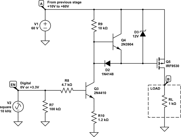
Then you need to switch the above adjustable source (at A) using a digital 0V/+3.3V signal:

schematic

simulate this circuit

When input EN is high (+3.3V), the output at B is enabled and connected to A. EN low (0V) will switch off Q5, disconnecting B from A.

This time the pass transistor Q5 is connected common-source, because we don't need linearity. To switch Q5 off, it requires a gate potential that rises all the way to \$V_A\$, which is the job of Q4. I don't use a simple pull-up resistor for that, because there's no value that would work well for low \$V_A\$, and which wouldn't draw excessive current at high \$V_A\$. Q3 pulls Q5's gate potential down to switch it on, while D3 limits \$V_{SG}\$ to 12V maximum. Q3's emitter is degenerated by R10 to limit collector current to a couple of milliamps, even when \$V_A=+60V\$. Q3 and Q5 will be handling 60V, so they are high-voltage types. Q5 is a power transistor, potentially dissipating 3W, so give it a heat-sink.

That's as simple as I can make it without knowing more about your application. There's no current limiting, or any other fail-safe mechanisms in place to protect the circuit from you or the load, and I make no guarantees about it at all. It's just a starting point, one possible solution, and possibly even useful. It will definitely need tweaking.

\$\endgroup\$
2
  • \$\begingroup\$ This is a great approach if efficiency is not a priority (Q2 will waste power when you want low voltage pulses). \$\endgroup\$
    – Mattman944
    Commented Nov 25 at 21:27
  • \$\begingroup\$ @Mattman944 Yes, agreed! I toyed with the idea of a DAC programmable boost converter too, because of this. That would also solve the poor transient response of my linear version above, but it's too deep a topic, so I stuck with linear. Maybe the wrong choice. \$\endgroup\$ Commented Nov 26 at 3:30
2
\$\begingroup\$

You should create a solid target voltage first. A discharge will not meet your pulse shape requirements.

Worst case current is 60V/10k = 6mA. You should be able to do this with a boost converter.

You need a feedback loop. Digital or Analog?

A digital control loop will use less parts, and your loose specs should allow a low loop frequency. Don't try to design your own algorithm, use a known PID algorithm. One of the contributors here has a good tutorial online, https://www.wescottdesign.com/articles/pid/pidWithoutAPhd.pdf

An analog loop should allow you to buy a SMPS IC. The MCU will need to drive a DAC for the set voltage. An MCU PWM output followed by a low-pass filter will create a basic DAC. It may be suitable for your needs.

For the output stage, you probably need to switch the high-side. To do this you need a level-shifter (N-MOSFET), followed by a P-MOSFET that switches the voltage to the load.

\$\endgroup\$
1
\$\begingroup\$

You can simply use 2 boost converters in series. The first one boosts the 3V to something around 24-30V. The second one boosts the output of the first to 60V. You could probably even use the microcontroller to get a variable 12-60V output from the 2 converters.

\$\endgroup\$
1
  • 1
    \$\begingroup\$ Strictly speaking, this is more "cascade" than "series". \$\endgroup\$
    – Hearth
    Commented Nov 25 at 0:29
1
\$\begingroup\$

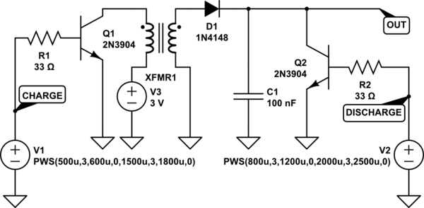
Here is a solution where the transformer discharge pulse goes directly into the output. It uses two pins on your microcontroller, one for the charge pulse and the other for returning the output to zero.

By changing the pulse width of the charge signal, you control the amount of energy that is stored and released by the transformer. This energy pulse then charges a capacitor of known capacity, which converts energy into voltage and maintains that voltage. The discharge control signal discharges the capacitor and returns the output to zero.

schematic

simulate this circuit – Schematic created using CircuitLab

\$\endgroup\$

Your Answer

By clicking “Post Your Answer”, you agree to our terms of service and acknowledge you have read our privacy policy.

Not the answer you're looking for? Browse other questions tagged or ask your own question.