1
\$\begingroup\$

I have a NAND logic gate, the top 6 pins appear to be working fine (4x Input, 2x Output) However the bottom 6 pins on the IC appear not to work.

I was testing the IC via an LED, connecting two high currents to the input and then the output to the LED, it works fine for the top half and not for the bottom.
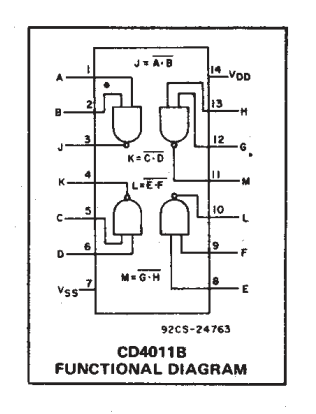
enter image description here

In relation to the pin map above, I have tried pins KCD, LFE, placing a high current into pins C & D expecting a high input from K and also E & F expecting a high input from L.

Is the IC damaged or am I missing something?

The IC is a Texas Instruments CD4011B

Data Sheet: http://www.ti.com/lit/ds/symlink/cd4011b.pdf

Jacob.

\$\endgroup\$
7
  • 1
    \$\begingroup\$ When testing the "upper" gates, did you tie unused "lower" inputs to VSS/VDD? Did you follow any anti-static precautions when handling the chip? \$\endgroup\$ Commented Jul 5, 2013 at 10:02
  • \$\begingroup\$ I left the 5v and GND power to the chip in at all times. When testing the upper parts I used pull down resistors to GND on the two HIGH input NANDs \$\endgroup\$ Commented Jul 5, 2013 at 10:04
  • \$\begingroup\$ 1) When testing A,B you also need to connect G,H, C,D, E,F to 5V or GND. 2) Since the chip's datasheet suggests it's outputs can only handle a few milliamps, it may be unwise to use them to power a LED at 10 or 20 mA. \$\endgroup\$ Commented Jul 5, 2013 at 10:15
  • 1
    \$\begingroup\$ "With the inputs disconnected, the gates may be biased into a mode where the outputs are partially conducting; this leaves the output buffer drawing a great deal of current since it is not fully on or off, creating a low resistance current path between the power supply rails." - Wikipedia \$\endgroup\$ Commented Jul 5, 2013 at 10:24
  • 1
    \$\begingroup\$ What are the "top" and "bottom" pins of an IC? I have not heard of this concept. Why don't you just name which pin numbers you think are working and which aren't? Obviously, VDD and VSS must be working, and they are in opposite corners of the IC. \$\endgroup\$
    – Kaz
    Commented Jul 5, 2013 at 15:05

1 Answer 1

3
\$\begingroup\$

My guess is that the chip has been damaged by electrostatic discharge or by overcurrent.

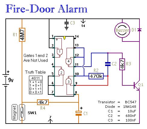
That CMOS chip's datasheet suggests it's outputs can only handle a few milliamps, not enough to drive a typical 20mA LED directly. Here is an example circuit.

enter image description here

Note that inputs on unused gates are tied to VSS or VDD

Note that a transistor is used to drive the load.

\$\endgroup\$
4
  • \$\begingroup\$ Thanks, so if the IC cannot drive the LED, what should I be using to drive it? \$\endgroup\$ Commented Jul 5, 2013 at 10:29
  • 1
    \$\begingroup\$ One way is to use a NPN transistor with a 4.7 kΩ resistor to limit base current and (say) a 220 Ω resistor to limit collector current. \$\endgroup\$ Commented Jul 5, 2013 at 10:40
  • \$\begingroup\$ So to summarise, in future I should always tie down unused INPUTS on an IC and I should ALWAYS use a transistor to drive the output and not the IC directly? \$\endgroup\$ Commented Jul 5, 2013 at 10:44
  • 1
    \$\begingroup\$ @Jacob: "ALWAYS" is a bit too categorical, but it won't hurt during testing. \$\endgroup\$ Commented Jul 5, 2013 at 10:48

Your Answer

By clicking “Post Your Answer”, you agree to our terms of service and acknowledge you have read our privacy policy.

Not the answer you're looking for? Browse other questions tagged or ask your own question.