I want to have a square wave that goes from 0 VDC to 5VDC go through some sort of amplifier and that amplification takes that same wave ( at a frequency of 1200Hz but could also be adjusted later ) but now makes it 0VDC to 13VDC (at least 13VDC, it could be 13.4 VDC, but not lower than 13VDC). The original wave would be generated from a function generator, but I do not want to exceed 5VDC. How would I got about doing this?
-
1\$\begingroup\$ what power supply is available? \$\endgroup\$– markragesCommented Aug 6, 2013 at 18:28
-
\$\begingroup\$ I have a 30VDC power supply, 3Amps of current available (its a variable one, so I can adjust to whatever). \$\endgroup\$– ProspectiveEngCommented Aug 6, 2013 at 18:34
-
\$\begingroup\$ Just to be sure, is there any negative power supply available? How close to zero do you need the output zero level to be? How much current will the output have to sink when it is at the zero level? (More generally, what is the load on the output?) \$\endgroup\$– The PhotonCommented Aug 6, 2013 at 18:49
-
\$\begingroup\$ No negative power supply available. The output should act like a short, so like as close as possible. The output should be able to handle at least 250 mA but I want to double that to be 500 mA, to be safe. I'm trying to simulate packets of data for DALI protocol. \$\endgroup\$– ProspectiveEngCommented Aug 6, 2013 at 19:55
3 Answers
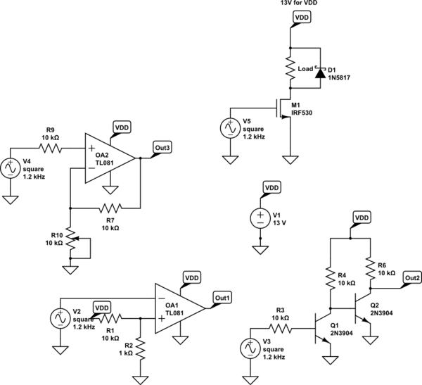
There are many methods to approach this. You can adjust your power supply to 13V and use an opamp as a comparator (Out1) or use a two stage npn amplifier (Out2) to amplify your signal. If you want to adjust gain but not your power supply, then use a non-inverting opamp gain (Out3).
How each works:
When your signal is above VDD*R2/(R2+R1) = 13*1k/(1k+10k) = 1.18V, the opamp with its open loop gain is saturated. You're essentially making a switch, either on or off.
Your signal comes in. The cascaded stages of npn yield high gain. You can get away with one as the beta, gain factor, of the transistor is around 100.
Vo = Vin*(1 + R7/R10). Just turn the pot to adjust.
If you need high current output, then use a power opamp like a LT1210 from linear technology.

simulate this circuit – Schematic created using CircuitLab
-
\$\begingroup\$ I'm liking the NPN 2 stage transistor version, however those NPN transistors only handle roughly 200mA of current. I need to get a transistor with 13VDC capability of 250mA and just to be safe we'll double that to be 500mA. So could I just replace the 2 transistors with 2 different NPN transistors and it should be good or would the values of the resistors also have to change, since I'm assuming the beta will change for the new transistors? \$\endgroup\$ Commented Aug 7, 2013 at 16:20
-
\$\begingroup\$ Another thing if the output lets say draws out 250mA of current will that current becoming from the power supply or will it also come from the function generator? I'm still a beginner for transistor theory, haven't learned it yet in University, however I have an idea of how they work. Thank you so much though, this is a great solution. \$\endgroup\$ Commented Aug 7, 2013 at 16:23
-
\$\begingroup\$ @ProspectiveEng In that case, look at the updated schematic. Use a nmos to switch instead because of current drawn. Issue with npn is the heat dissipation. Power is calculated by P = IV = I^2*R. For NPN, it is IV = 500mA*0.7V = 350mW. For NMOS, it is I^2*Ron = (500mA)^2*10mOhms = 2.5mW. Just way more efficient. You can get nmos with Ron less than 5mOhms easily. \$\endgroup\$ Commented Aug 7, 2013 at 17:01
-
\$\begingroup\$ The solution at lower right has a problem. With R6 at 10 kOhms, it's not going to be able to supply 250 mA to the load when the output is "high". \$\endgroup\$ Commented Aug 7, 2013 at 17:40
-
\$\begingroup\$ The solution at upper right inverts the sense of the control signal (which might be no big deal). Also, I'm not seeing how it can sink 250 mA out of the load when its output is in the "0 V across the load" state. \$\endgroup\$ Commented Aug 7, 2013 at 17:41
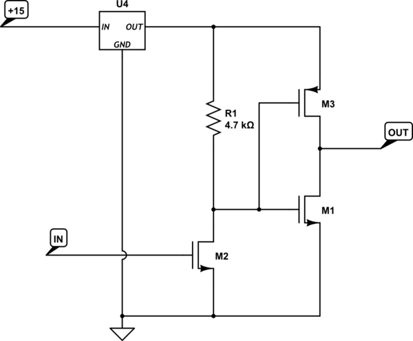
One way is to essentially build a couple of stages of digital inverter from discrete parts:

simulate this circuit – Schematic created using CircuitLab
U4 is a linear regulator programmed for 13 V output or a bit higher. Keeping the input power voltage close (but not too close) to 13 V will minimize power lost in the regulator.
The value of R1 can be varied to balance power consumption against switching speed.
Choosing actual part numbers for the FETs is left as an excercise for the reader. M2 needs to have low enough threshold voltage to be turned hard on by a 5 V input. M1 and M3 need to withstand ~15 V Vgs, and need to be able to carry your load current when "on".
Look up pnp multivibrator. It is an adjustable square wave circuit. You will need two pnp transistors 3906, 4403 or if you burn those up, you can still use 2907 at a lower amp input, two 100kohm two 2200ohm and two 100ohm transistors, two 1uf capacitors and two diodes and or LEDs. The frequency and voltage are increased by applying more 100kohm resistors in parallel to the base of either transistor, and decreased by either removing either 100kohm resistors from the base of either transistor or applying more capacitors to the emitter and base of opposing transistors. As for the heat problem you have with your transistors not being able to withstand the amperage, try using the same type of transistor in parallel meaning just add another transistor where the one with the same function is.
