4
\$\begingroup\$

Problem: I have a logic signal (represented by SW1), say from a microcontroller, that is either 0V or some low voltage, maybe 5V or 3.3V. I have a higher voltage supply (V1) and a switching device (M1) on the high side of that supply, connected to a load.

schematic

simulate this circuit – Schematic created using CircuitLab

Sometimes, there is an H-bridge, or half an H-bridge, and I need to control the high-side transistor(s) (M2), but I think basically it's the same problem:

schematic

simulate this circuit

The difficulty is that my logic output is only 0V or 5V, but I need higher voltages, like maybe 50V and 45V, to switch the high-side transistor. I understand that the precise voltages required will depend on the transistors I select -- I'm just wondering how to solve this problem, generally.

Is there a simple way to do this if my application is not very demanding? If I need to do the switching rapidly, say for a PWM application at 50kHz, is there a more complicated way to do it?

\$\endgroup\$
9
  • \$\begingroup\$ hint: I know the answer. I'm looking for a canonical answer for the FAQ. \$\endgroup\$
    – Phil Frost
    Commented Aug 14, 2013 at 14:41
  • \$\begingroup\$ Is your top diagram correct with the supply and load? Damn those strange symbols. \$\endgroup\$
    – Andy aka
    Commented Aug 14, 2013 at 14:47
  • \$\begingroup\$ @Andyaka err...is this right? These symbols always look wrong to me \$\endgroup\$
    – Phil Frost
    Commented Aug 14, 2013 at 14:54
  • \$\begingroup\$ Is this to use a high side driver application? \$\endgroup\$ Commented Aug 14, 2013 at 15:01
  • \$\begingroup\$ @EwokNightmares I'm not sure what you mean. \$\endgroup\$
    – Phil Frost
    Commented Aug 14, 2013 at 15:49

5 Answers 5

5
\$\begingroup\$

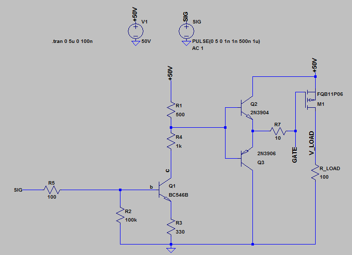
Aside from IC and isolated solutions (e.g. high side switch ICs, transformers, opto, etc - which is what you'd usually go for nowadays), one simple solution is a reasonably fast discrete PMOS driver circuit like this:

enter image description here

Obviously you can just use the one NPN version, but the push pull increases drive capability. This is just the rough idea, divider can be adjusted and protection added to ensure Vgs tolerance is met. Q1's emitter resistor is to prevent it saturating and lengthening the turn off time.

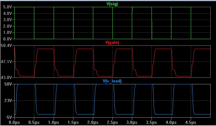
Simulation at 1MHz - I added the gate voltage (red trace), note it only swings ~7V, it follows the Q2/Q3 base voltage (a zener can be added as mentioned if needed):

enter image description here

\$\endgroup\$
4
  • 1
    \$\begingroup\$ I like it. I would think an important feature of the push-pull beyond speed is the fact that it looks as though it would limit the effect of gate-drain capacitance. Without that, I would think there could be situations where gate-drain capacitance could cause the gate-source to exceed the Absolute Maximum Rating. \$\endgroup\$
    – supercat
    Commented Aug 14, 2013 at 20:59
  • \$\begingroup\$ I think you'd need to float the driver circuit up to about 35V to avoid FET destruction via gate voltage overload. \$\endgroup\$
    – Andy aka
    Commented Aug 14, 2013 at 21:32
  • \$\begingroup\$ @Andy: see the gate trace, it doesn't drop to 0V - it follows the R1/R4 divider voltage. \$\endgroup\$
    – Oli Glaser
    Commented Aug 14, 2013 at 21:43
  • 1
    \$\begingroup\$ @OliGlaser so it does you clever person \$\endgroup\$
    – Andy aka
    Commented Aug 14, 2013 at 22:19
4
\$\begingroup\$

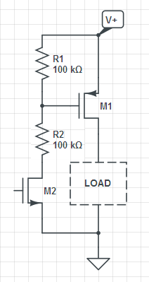
enter image description here How about a pull-up for the M1's gate (the P-FET) and an N-FET (M2) from that gate to ground? If you power M2 you pull M1's gate low, switching it on. If M2 is off the pull-up resistor ensures M1 is switched off.
More details: P-FET M1 is switched on if its gate becomes a few volts lower than the source (the arrow). ANd N-FET M2 is switched on if its gate becomes a few volts higher than the source. So if you apply a high voltage to M2's gate it will be on, pulling the gate of M1 low. This creates the required voltage drop between gate and source to switch M1 on. So applying a voltage to M2 will switch M1 on.
If you make the gate of M2 low it will switch off. Then the gate of M1 will be pulled high by R1, and there won't be a voltage difference between gate and source. Then M1 will switch off.

\$\endgroup\$
6
  • 1
    \$\begingroup\$ I don't really understand what you mean. Can you draw a schematic and explain how it works? I'm just learning electronics. \$\endgroup\$
    – Phil Frost
    Commented Aug 14, 2013 at 14:49
  • \$\begingroup\$ @PhilFrost: I added a schematic and more details about the working. \$\endgroup\$ Commented Aug 14, 2013 at 15:13
  • \$\begingroup\$ Will this pullup limit your allowable switching frequency? And for many high power applications, the MOSFET junction capacitances are large to charge with that 100kohm. \$\endgroup\$ Commented Aug 14, 2013 at 15:15
  • \$\begingroup\$ @EwokNightmares: I missed the PWM frequency in the question, but you're right. The resistor value must be much lower, maybe 1kohm (depends on the FET). \$\endgroup\$ Commented Aug 14, 2013 at 15:18
  • \$\begingroup\$ @PhilFrost: You would need a FET with \$V_{GS(max)}\$ of 50V, yes. I don't know how common these are. Alternatively you can add a resistor between the gate of M1 and M2, so that the resistors divide the 50V to a lower value. \$\endgroup\$ Commented Aug 14, 2013 at 15:53
1
\$\begingroup\$

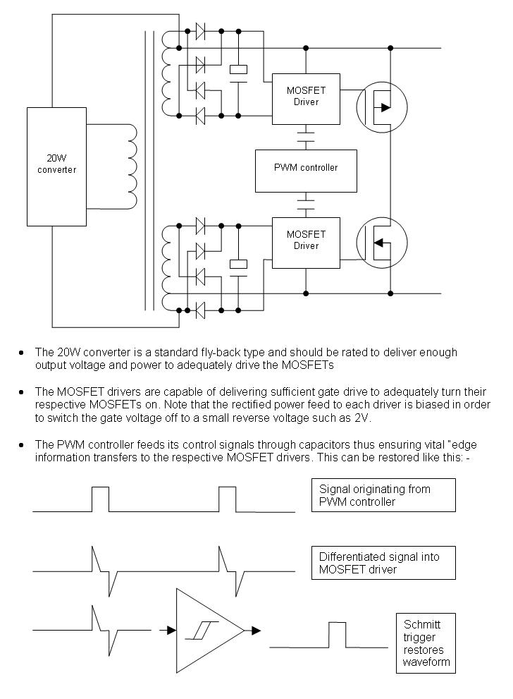
There are few basic solutions:

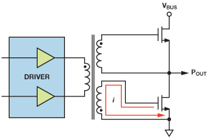
Gate transformer: you will be able to control both transistors in a leg with one transformer but the transformer itself may be hard to design.

enter image description here

Fully isolated gate drivers: simple but expensive solution as you will need to provide isolated power to high side gate driver(s). This means using expensive DC/DC converters or a transformer with multiple isolated secondary windings.

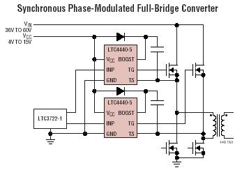
Bootstrap circuit: the boost capacitors provide power for high-side gate drivers. These caps are charged when low-side mosfet is on. This is a cheap solution but you must be sure to properly start-up the circuit. First turn-on all bottom mosfets to charge the boost caps. Only then can you properly start the converter.

enter image description here

\$\endgroup\$
3
  • \$\begingroup\$ This is my favourite answer. For a start the LTC4440 is an awesome chip and will, apply equal delays to both top and bottom fets thus not forcing a significant conduction overlap. Plus I'd still go for a transformer drive because it can drive P channel or N channel with a few refinements not shown in the above. \$\endgroup\$
    – Andy aka
    Commented Aug 14, 2013 at 22:26
  • 1
    \$\begingroup\$ Neat, but all these are using N-channel FETs on the high side. I'm using P-channel FETs in the question. \$\endgroup\$
    – Phil Frost
    Commented Aug 15, 2013 at 11:51
  • \$\begingroup\$ With these gate driver circuits you do not have to use Pfets. You can adapt them all, or even simplify them (see Oli's answer and app note AN-940 from IR), to suit high side Pfet. But in reality Nfets are much better and it is worth adding some complexity in gate circuit to have a all Nfet design. Smaller BOM and smaller losses are realy worth it. \$\endgroup\$ Commented Aug 15, 2013 at 15:08
0
\$\begingroup\$

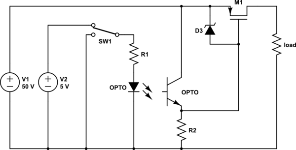
If you don't need a very high switching speed, an optocoupler will do the trick. If the switching voltage is high, you might need a zener diode to make sure you don't exceed the Vgs spec for the FET.

schematic

simulate this circuit – Schematic created using CircuitLab

\$\endgroup\$
1
  • 1
    \$\begingroup\$ With this circuit, if there's a fault that causes you to lose power on the low voltage side, the switch will fail closed. Which is cool if that's what you want, but I'd guess it's more common to want the switch to fail open. \$\endgroup\$
    – The Photon
    Commented Aug 15, 2013 at 15:28
0
\$\begingroup\$

I'm going for the high power and fast PWM end of the question because its the most difficult to solve as a design. I deleted yesterday's answer not because it was wrong but because this is a more refined idea: -

enter image description here

After the schmitt trigger has restored the control waveforms I'd use a standard push-pull MOSFET driver and, due to the slight asymmetry in the rails it will produce (say) a 12V active drive to the gate with a 2V reverse drive for switching the gate off quickly.

I would use the same driver topology on both FETs so that any delays are equal to both top and bottom FETs.

\$\endgroup\$

Your Answer

By clicking “Post Your Answer”, you agree to our terms of service and acknowledge you have read our privacy policy.

Not the answer you're looking for? Browse other questions tagged or ask your own question.