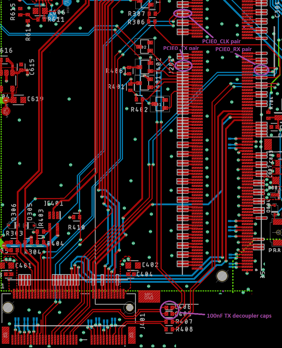
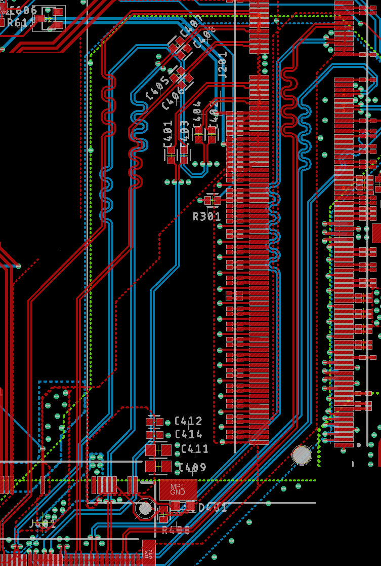
I have designed an custom NVIDIA Jetson carrier board based on P3449-B01 Jetson Nano Carrier Board reference design by NVIDIA.
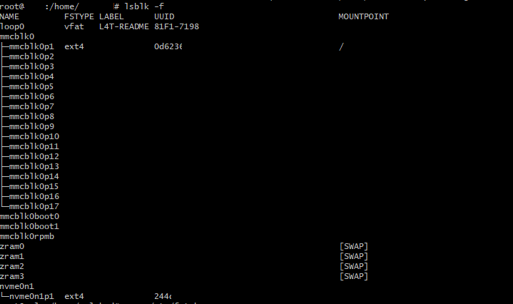
The carrier board is working fine, the linux is booting up, however when I attach an x1 PCIE device (NVME on x1 PCIE lane) the linux is not booting up.
I tried to track down the issue with journalctl but when I use the following command: journalctl --list-boot
it does not list the failed boot sequence.
My testing procedure:
- Power the device from external DC source
- Wait until my router assigns IP to the device
- login into linux through SSH over ethernet
- check dmesg or do any kind of testing
If I do these steps without PCIE device, all steps can be done. If I do it with the NVME attached it stucks at step 2. Router does not assign IP.
I have tested the on board PSU, it is tested to drive 2.5-3A current from 5V, and it is capable to drive upto 5A. In idle without NVME the NVDIA draws approx. 400mA current, with NVME it draws 700-800mA so I don't think it is PSU issue. Based on the current consumption, it tries to do something when the NVME is connected, but I cannot connect to the device to check dmesg...
I have double checked the wiring of the PCIE lines, all looks OK to me. PCIE lanes are routed differentially, matched to 90ohms on a 4 layer board. My last thinking probably it is related to signal integrity issue, but in this case still I should have a working linux system.
Any idea how to track down the PCIE issue?
UPDATE:
For suggestion of Ron Beyer I examined the problem on the debug serial terminal, where the boot messages can be read. With the SSD when it starts the kernel it drop plenty of error messages for the PCIE bus. Such as:
[    1.558693] pcieport 0000:00:01.0: PCIe Bus Error: severity=Corrected, type=Physical Layer, id=0008(Receiver ID)
[    1.581631] pcieport 0000:00:01.0:   device [10de:0fae] error status/mask=00000001/00002000
[    1.600096] pcieport 0000:00:01.0:    [ 0] Receiver Error         (First)
[    1.629938] pcieport 0000:00:01.0: PCIe Bus Error: severity=Corrected, type=Physical Layer, id=0008(Receiver ID)
[    1.645772] pcieport 0000:00:01.0:   device [10de:0fae] error status/mask=00000001/00002000
[    1.658393] pcieport 0000:00:01.0:    [ 0] Receiver Error         (First)
[    1.682121] pcieport 0000:00:01.0: PCIe Bus Error: severity=Corrected, type=Physical Layer, id=0008(Receiver ID)
[    1.695462] pcieport 0000:00:01.0:   device [10de:0fae] error status/mask=00000081/00002000
[    1.705945] pcieport 0000:00:01.0:    [ 0] Receiver Error         (First)
[    1.706543] pcieport 0000:00:01.0:    [ 7] Bad DLLP
[    1.708031] nvme 0000:01:00.0: PCIe Bus Error: severity=Corrected, type=Data Link Layer, id=0100(Transmitter ID)
[    1.708799] nvme 0000:01:00.0:   device [126f:2263] error status/mask=00001000/0000e000
[    1.709177] nvme 0000:01:00.0:    [12] Replay Timer Timeout
[    1.718745] pcieport 0000:00:01.0: PCIe Bus Error: severity=Corrected, type=Physical Layer, id=0008(Receiver ID)
[    1.721020] pcieport 0000:00:01.0:   device [10de:0fae] error status/mask=00000001/00002000
[    1.721495] pcieport 0000:00:01.0:    [ 0] Receiver Error         (First)
And after couple of secs these repeated errors are replaced with:
[    2.133600] pcieport 0000:00:01.0:   device [10de:0fae] error status/mask=00000001/00002000
[    2.136428] pcieport 0000:00:01.0:    [ 0] Receiver Error         (First)
[    2.138200] pcieport 0000:00:01.0: PCIe Bus Error: severity=Corrected, type=Physical Layer, id=0008(Receiver ID)
** 4 printk messages dropped ** [    2.144891] pcieport 0000:00:01.0: PCIe Bus Error: severity=Corrected, type=Physical Layer, id=0008(Transmitter ID)
** 15 printk messages dropped ** [    2.158376] pcieport 0000:00:01.0: PCIe Bus Error: severity=Corrected, type=Physical Layer, id=0008(Receiver ID)
** 9 printk messages dropped ** [    2.165170] pcieport 0000:00:01.0:    [ 0] Receiver Error         (First)
** 7 printk messages dropped ** [    2.171578] pcieport 0000:00:01.0:   device [10de:0fae] error status/mask=00000001/00002000
** 8 printk messages dropped ** [    2.182061] pcieport 0000:00:01.0:    [ 0] Receiver Error         (First)
** 8 printk messages dropped ** [    2.196782] pcieport 0000:00:01.0:    [ 0] Receiver Error         (First)
** 8 printk messages dropped ** [    2.205280] pcieport 0000:00:01.0: PCIe Bus Error: severity=Corrected, type=Physical Layer, id=0008(Receiver ID)
** 6 printk messages dropped ** [    2.221748] pcieport 0000:00:01.0: PCIe Bus Error: severity=Corrected, type=Physical Layer, id=0008(Receiver ID)
** 7 printk messages dropped ** [    2.229780] pcieport 0000:00:01.0: PCIe Bus Error: severity=Corrected, type=Physical Layer, id=0008(Receiver ID)
** 9 printk messages dropped ** [    2.248932] pcieport 0000:00:01.0: PCIe Bus Error: severity=Corrected, type=Physical Layer, id=0008(Receiver ID)
** 6 printk messages dropped ** [    2.256010] pcieport 0000:00:01.0: PCIe Bus Error: severity=Corrected, type=Physical Layer, id=0008(Receiver ID)
** 5 printk messages dropped ** [    2.263474] pcieport 0000:00:01.0:    [ 0] Receiver Error         (First)
** 3 printk messages dropped ** [    2.269535] pcieport 0000:00:01.0:    [ 0] Receiver Error         (First)
** 3 printk messages dropped ** [    2.278270] pcieport 0000:00:01.0:    [ 0] Receiver Error         (First)
** 6 printk messages dropped ** [    2.284579] pcieport 0000:00:01.0: PCIe Bus Error: severity=Corrected, type=Physical Layer, id=0008(Receiver ID)
** 11 printk messages dropped ** [    2.296427] pcieport 0000:00:01.0:   device [10de:0fae] error status/mask=00000001/00002000
** 11 printk messages dropped ** [    2.312921] pcieport 0000:00:01.0:   device [10de:0fae] error status/mask=00000001/00002000
** 4 printk messages dropped ** [    2.313943] pcieport 0000:00:01.0:    [ 0] Receiver Error         (First)
** 9 printk messages dropped ** [    2.333645] pcieport 0000:00:01.0: PCIe Bus Error: severity=Corrected, type=Physical Layer, id=0008(Receiver ID)
** 9 printk messages dropped ** [    2.352748] pcieport 0000:00:01.0:    [ 0] Receiver Error         (First)
I guess that is the PCIE bus error which comes from the PCIE lanes wiring?


