0
\$\begingroup\$

I'm laying out an ESC (sorry can't post photos) and I'm trying to squash any noise on the board. I unfortunately have limited space which requires me to run LV signal traces from my current sense amplifiers under the drive FETs. I do have a 10-layer board, but need 6 layers to carry the necessary current to from the phase outputs of the FETs to the motor wires. My plan was to make layer 7 the return path. This leads me to 2 or 3 questions:

  1. My current amplifier output traces are on layer 8, below the return plane, which is below the phase outputs. Is that sufficient to prevent noise interference on the LV traces from the outputs of the FETs?

  2. The ESC also reads voltage feedback from each phase. This is divided down before it is read by the ADC. Should I put the resistive dividers close to the FETs and run LV traces (same layer as the current feedback) back to the ADC, or should I run HV traces to the divider which is close to the ADC, but will bring HV traces near the processor?

  3. Is one layer of return path (plane essentially) sufficient to block switching noise?

Does anyone have a good reference on laying out ESC PCBs? I could use a good guide if one exists.

\$\endgroup\$
6
  • \$\begingroup\$ What’s your stack up? Which layers have what on them? Is opening the soldermask layers on the outer layers an option for you to get lower resistance? \$\endgroup\$
    – winny
    Commented Feb 17, 2023 at 21:39
  • 3
    \$\begingroup\$ With out schematic, layer stack, and seeing what you have done layout wise this is pretty near impossible to answer. At least in my opinion :) \$\endgroup\$ Commented Feb 17, 2023 at 21:58
  • \$\begingroup\$ @RogerDodger - I'm doing the best I can, but I'm prohibited from sharing the schematic and layout. \$\endgroup\$ Commented Feb 17, 2023 at 22:41
  • \$\begingroup\$ @winny - opening the soldermask isn't an option. My stackup is 10 layer 093, but nothing is set in stone yet. I'm just starting to lay copper now. Currently, power devices on top layer, digital electronics on the bottom layers wherever possible. I'm reserving layer 7 as a ground plane. \$\endgroup\$ Commented Feb 17, 2023 at 22:43
  • 1
    \$\begingroup\$ @JediEngineer, your last comment there saying laying out digital electronics where ever, probably isn't a good approach. For EMC/SI/PI, stackup and circuit and component placement play a very important role. I don't know your experience, or the circuit, or, anything your really doing, but, really focus on placement, routing signals where there references are (1 dielectric away) and, really thinking about your return currents. Not routing current sense lines return path through the switched 400V 10A path. Stuff like that \$\endgroup\$ Commented Feb 17, 2023 at 22:51

1 Answer 1

1
\$\begingroup\$

I am no expert on PCB layout, but I can show you a typical example of a brushless 'hobby' ESC. This one was made by Castle Creations in the US.

It is a 4 layer board with the logic on one side and the FETs on the other. Both middle layers are (mostly) ground, but separate from each other except where the negative power lead is connected. So it is effectively two 2 layers boards sandwiched together (some ESCs do the same thing with two separate boards).

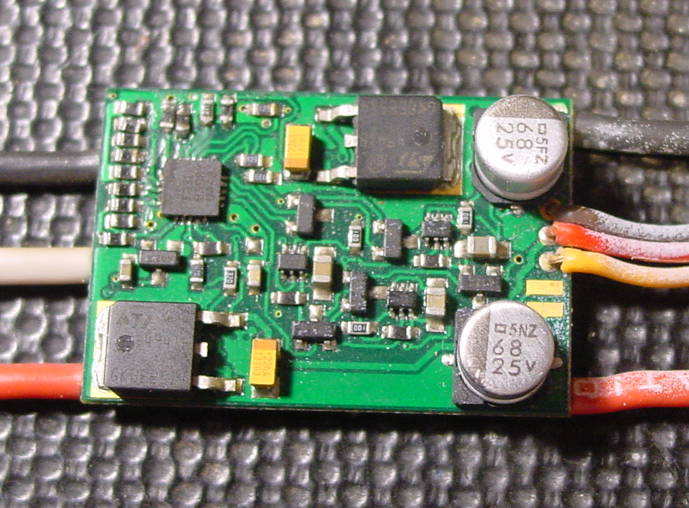
First the logic side. Here we have:-

  • Top left: column of resistors creating the voltage dividers and virtual neutral point. Inputs through vias from phases on other side, outputs going into the MCU immediately to the right of them.

  • Middle area: FET drivers.

  • Right: power inputs (through vias from power input wires on other side), bulk capacitors, gnd/+5V/signal wires to receiver.

  • Bottom left, top middle/right: +5 V linear regulators for MCU and receiver/servos.

enter image description here

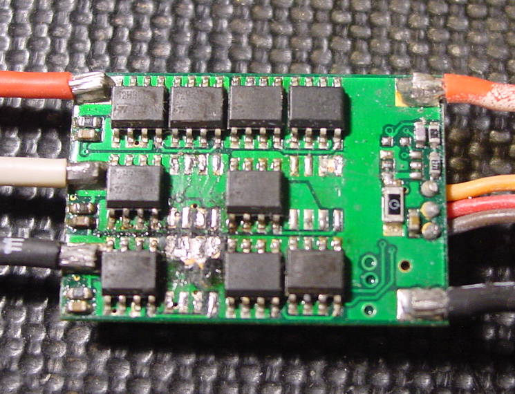
Now the other side (ignore messy part where some FETs were removed, all the FETs in this ESC are burnt!):-

  • Left: motor phase wires, snubbers between adjacent phases.

  • Middle: FETs. Lower FETs to the left, Sources connected to Negative (gnd) on inner layer. Upper FETs to the right, Drains connected to Positive on top layer.

  • Right: Power input wires, signal filtering components (from orange wire), unpopulated area for opto-coupler option.

enter image description here

The two inner ground layers being separate isolates the sensitive analog and logic parts from high currents flowing in the tracks on the FET side, and shields them from any EMI radiating from the tracks (which shouldn't be much if the switching times are well controlled).

As you have more layers you have more freedom to route signal wires on inner layers without compromising the ground plane. Depending on motor current, you may want to combine several layers to reduce resistance on the FET side.

\$\endgroup\$

Your Answer

By clicking “Post Your Answer”, you agree to our terms of service and acknowledge you have read our privacy policy.

Not the answer you're looking for? Browse other questions tagged or ask your own question.