0
\$\begingroup\$

I am very new to electronics and just started learning about logic gates.

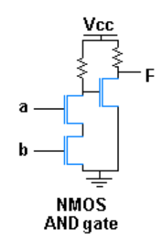
I read about the AND gate and learned about its boolean algebra, but I also wanted to make one myself using MOSFETs which I learned about earlier. The AND-gate I made was pretty much identical to the one in picture 1. The only difference is that mine was implemented in an entire circuit. But I will use this picture because it's simpler and illustrates the problem more clearly.

Picture off AND-gate made by only NMOS-transistors

Not sure if this was a good (or best) way to create an AND-gate using MOSFETs I started looking on the web for optimal constructions. Then I found this earlier post on engineering exchange which is very much a similar question to mine. However, it did not help me because I did not actually understand the explanations. This is because the explanation was meant for people with more advanced knowledge.

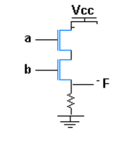
There is a picture of the AND-gate with the inverter below:

The AND-gate which also includes a inverter

Here are my questions:

  1. Could you explain to a less knowledgeable person in electronics why the AND-gate is improved by adding the inverter?

  2. Is this inverter trick normally used in other types of logic-gates?

  3. Is this AND-gate design using the inverter considered the "best AND-gate design" or are there multiple different designs for different use cases?

  4. This is somewhat similar to question 3: Is there a generally considered best design for all the different logic gates? Is there a way to prove logic-gate design x is more efficient than all the other ones? Or does it mostly come down to price when producing them as long as it gets the job done?

\$\endgroup\$
10
  • \$\begingroup\$ What are you referring to as the "inverter component"? There is a part of that circuit that I would call an inverter, but it's not made of "two resistors". \$\endgroup\$
    – Hearth
    Commented Sep 6, 2023 at 21:01
  • \$\begingroup\$ @Hearth, The author of the post-question I linked asked why there was "an additional inverter part" in the logic gate. I thought I was referring to the two resistors. Am I incorrect? \$\endgroup\$
    – volticus
    Commented Sep 6, 2023 at 21:05
  • 2
    \$\begingroup\$ You've mistakenly identified what part of this is the inverter. The inverter is not the two resistors at the top; the inverter is the resistor and MOSFET on the right. "Inverter" here means the same thing as "NOT gate." As far as I know, that's an ordinary NMOS NOT gate. \$\endgroup\$ Commented Sep 6, 2023 at 21:06
  • \$\begingroup\$ Yes, and AND gate is made using a NAND gate plus a NOT gate. NOT gates are also called inverters. \$\endgroup\$ Commented Sep 6, 2023 at 21:09
  • 3
    \$\begingroup\$ The problem with your AND gate is the output voltage is lower than the input voltage. If you connected the output to another gate, the second gate's output would be even lower. After a few gates the voltage would always be 0 so the gates wouldn't work. A good gate has to make sure the output voltage is at least as good as the input voltage (closer to Vcc when high, closer to 0V when low). \$\endgroup\$ Commented Sep 6, 2023 at 21:09

1 Answer 1

1
\$\begingroup\$
  1. It's an AND gate made with NMOS transistors. You can't make an AND gate unless you invert the output of a NAND gate, and you can't do an AND gate directly with NMOS transistors.

  2. Yes, either on inputs, or output, or both, to build the logic function you want. For example for the same reason, you can do an NMOS NOR gate and invert the output to build an OR gate, because you can't build an OR gate directly with NMOS transistors.

  3. If you only want an AND gate that works in isolation, it is the most simple circuit that happens to work adequately so that why it is the best. If you are building a complex logic equation with a lot of inputs and intermediate results, you use the simplest circuit that does the task adequately, and you would not draw separate instances of separate logic gates, because it's wasteful to add transistors that could be simplified away.

  4. The best way is to use just the amount of circuitry needed to perform the needed logic function. You can't simplify a chip which needs to provide AND gates, but you can simplify a chip that needs to do a complex logic function with multiple inputs.

And what you might now be aware is that this only talks about NMOS logic, similar rules apply to PMOS logic, for CMOS the NAND gate would have both NMOS and PMOS transistors and inverter has two. And these are for static logic devices, if you have a system with a clock signal, you can make a more efficient system with less transistors if you use dynamic logic.

\$\endgroup\$
2
  • \$\begingroup\$ OK, thank you for the answer. But what stops the current from just going through the right resistor at the very top and out through F? Is the resistance of this resistor supposed to be very high so the current takes the long way around? Is the resistance on the left resistor supposed to be very low and why? Or does the power source have its plus side turned towards the left? And the illustration of the power source just shows this in another way. \$\endgroup\$
    – volticus
    Commented Sep 7, 2023 at 8:07
  • \$\begingroup\$ These are FETs. At this level of understanding basic logic gates, will be no current through the FET gate. And you have NMOS, so if you want to use NMOS transistors as high side switches, and you want to turn it on so that it outputs VCC, you have to bring the gate higher than VCC, and you don't have logic levels other than 0V and VCC. \$\endgroup\$
    – Justme
    Commented Sep 7, 2023 at 8:37

Your Answer

By clicking “Post Your Answer”, you agree to our terms of service and acknowledge you have read our privacy policy.

Not the answer you're looking for? Browse other questions tagged or ask your own question.