That data sheet is a wrong IMHO but first, a bit of background. The device you are wanting to know about is a P channel JFET and these types of transistor conduct drain current when there is zero gate-source voltage. To turn the device off you raise the gate-source voltage positively. For an N channel JFET you would raise the gate-source voltage negatively.
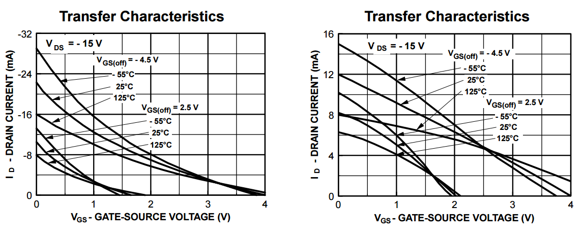
So let's look at the first two graphs in the OP's question: -

They shows typical characteristics for one device that has a VGS(off) voltage of 4.5 volts and the other characteristic is for a device with a VGS(off) voltage of 2 volts. It makes a mistake (IMHO) in that the 4.5 volt device appears to be listed as having a VGS(off) voltage of -4.5 volts - if it were it would be an N channel JFET and not a P channel JFET. So, that is there first mistake I believe.
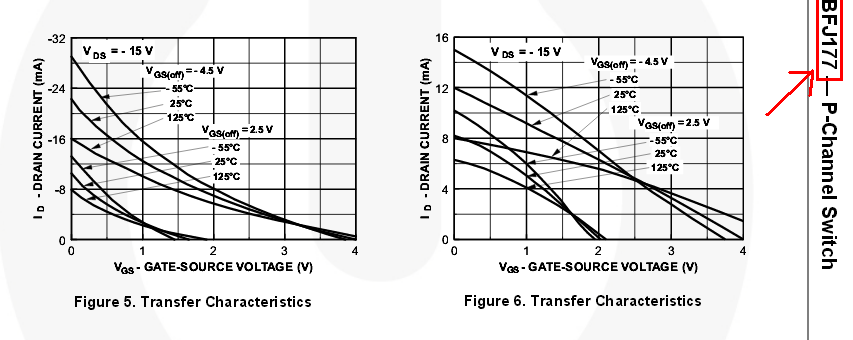
It also looks like this device has exactly the same characteristic as the J177 P channel mosfet - the graphs are identical as far as I can tell and I suspect that Fairchild may have dropped a major clanger: -

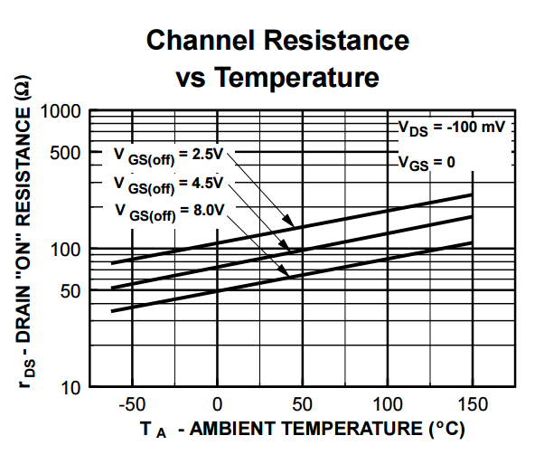
So back to the front page and the specification in the table is incomplete in my opinion. Using the J177 as an example, it lists a range of JFETs that are basically the same device but, due to manufacturing process variations have different VGS(off) voltages: -
- The J175 has a range of 3V to 6V for VGS(off)
- The J176 has a range of 1V to 4V for VGS(off)
- The J177 has a range of 0.8V to 2.5V for VGS(off)
In all other specifications they are the same device.
So here's the rub - the MMBFJ271 exists and has a VGS(off) value ranging from 1.5 volts to 4.5 volts.
Shame on Fairchild!
