2
\$\begingroup\$

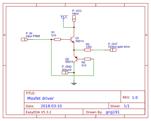
Im trying to drive mosfet's gate with couple of BJTs: S9014 (npn) and S9015 (pnp). They are in half bridge, VCC is 12V. Here is schematic:

Schematics

Input is PWM with frequency of ~70KHz from STM32 micro. I expect PWM from 0 to 12V on output, but strange thing happens instead: connecting 12V to VCC does almost nothing, PWM is still 0-3.3V with weird form and small DC offset (output was connected only to oscilloscope probe).
Question: Is my schematic correct and what is wrong with it?

\$\endgroup\$
16
  • 1
    \$\begingroup\$ Q1 is merely emitter-following your input PWM. What else should you expect? \$\endgroup\$
    – jonk
    Commented Mar 10, 2018 at 22:43
  • \$\begingroup\$ define your goal with Vout output and current limit. You only get Vbe drops from 3.3 giving 0.7 to 2.6 out \$\endgroup\$
    – D.A.S.
    Commented Mar 10, 2018 at 22:50
  • \$\begingroup\$ @jonk, I am expecting amplified 0-12V signal on output, how I can achieve this? \$\endgroup\$ Commented Mar 10, 2018 at 23:01
  • \$\begingroup\$ @GrigBetsan Not by emitter-following. That's for certain. You will have one BE drop from your MCU voltage rail, at best, at the output. You must modify your topology. And given the 70+ kHz you want, you must start to look more at parasitics, too. 100 kHz isn't hard. But it is moving into the area where lots of other considerations factor in. The slew rates start looking pretty darned fast. \$\endgroup\$
    – jonk
    Commented Mar 10, 2018 at 23:02
  • \$\begingroup\$ V Gain required<4 , level shift required. Wrong topology \$\endgroup\$
    – D.A.S.
    Commented Mar 10, 2018 at 23:06

2 Answers 2

3
\$\begingroup\$

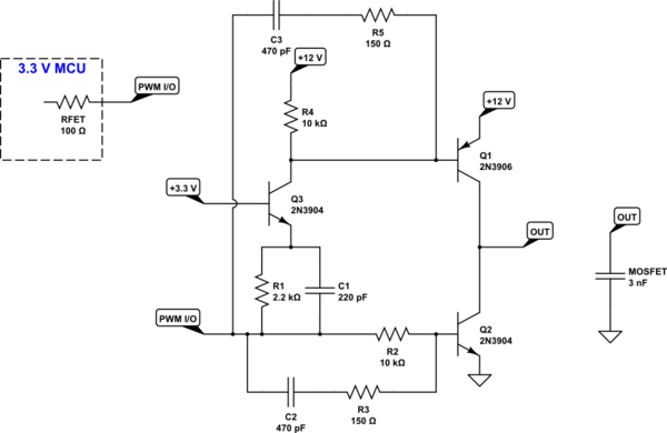
Here's a crafted design (except that I kind of ... roughed out ... the speed-up paths.) I am not worried about base oscillation of cascode \$Q_3\$ here, so I didn't do anything for it. It should be fine. If it turns out to be a problem, insert a \$68\:\Omega\$ to \$220\:\Omega\$ resistor between the base of \$Q_3\$ and the \$3.3\:\text{V}\$ supply rail.
schematic

simulate this circuit – Schematic created using CircuitLab

Worst case dissipation of any of the BJTs is probably under \$50\:\text{mW}\$, so they should be fine in open air as TO-92s. Perhaps a \$10^\circ\text{C}\$ rise?

Not shown, but probably needed will be some bypass capacitance -- I'd start with \$100\:\mu\text{F}\$ -- across the emitters of \$Q_1\$ and \$Q_2\$. Use short wiring, keep it tight, and probably use dead-bug style wiring.

Rise and fall times, of the circuit itself, can be kept near \$200\:\text{ns}\$, I believe. I would not expect worse than \$350\:\text{ns}\$, even with junk box parts. However, your MCU will have something to say about it as it's own I/O will slew at a rate of its own, too. But the edges are usually reasonably fast. I suspect this circuit will match up nicely.

\$\endgroup\$
20
  • \$\begingroup\$ cool! Could you give me a hint what the purpose of C2-R3 is? \$\endgroup\$ Commented Mar 11, 2018 at 0:20
  • 1
    \$\begingroup\$ @MarcusMüller Just a little speed-up to the base of \$Q_2\$ to sharpen the falling output edge. They are tricky because they work both ways and slow down the other edge -- though the active BJT wins out anyway. This is why I said I just "cheated" on the top and bottom speed-ups. I really should have sat down and spent more time on both of them. But I didn't want to, so I didn't. But these are used to pull charge out of the BJT, since they are operated "saturated." The cap is sized just big enough to get that job done for the BJTs you choose. \$\endgroup\$
    – jonk
    Commented Mar 11, 2018 at 0:32
  • 1
    \$\begingroup\$ ah, that makes sense. Also, looking at what it does explains pretty nicely why dead bug style is preferable – excessive parasitic inductivity would just lead to none of the transistors ever fully switching off \$\endgroup\$ Commented Mar 11, 2018 at 0:41
  • \$\begingroup\$ @MarcusMüller That reminded me to add the dead-bug wiring note to the answer, rather than leaving it in comments. Thanks! \$\endgroup\$
    – jonk
    Commented Mar 11, 2018 at 0:45
  • \$\begingroup\$ C1 is a 2.2us hammer driver on the output with 1A into 10 It can be reduced to match the FET requirements and add series R 200 Ohms to PWM input to raise output Rce. Similarily C2 is 70us can be reduced to 100ns \$\endgroup\$
    – D.A.S.
    Commented Mar 11, 2018 at 0:47
0
\$\begingroup\$

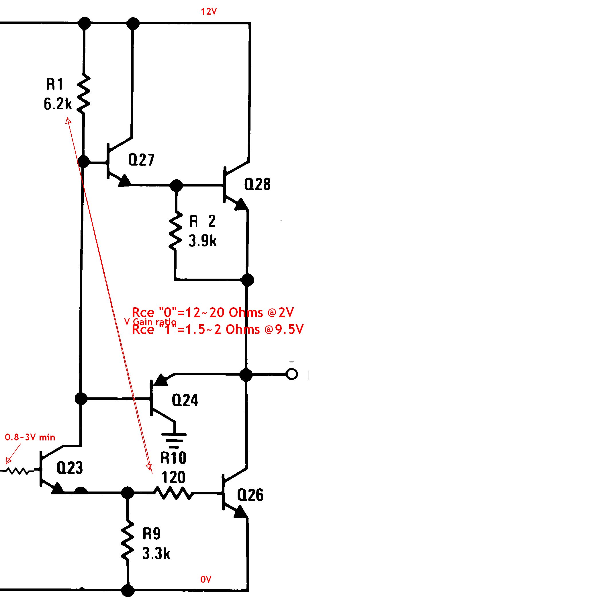
This is just one approach using an LM555 output driver.

There are existing CMOS FET drivers that are better. eg MIC4451 https://www.mouser.com/ds/2/268/mic4451-779120.pdf

enter image description here

Rce is the term I use to define Vol/Iol at 250 mA or (Vcc-Voh)/Ioh

with f(-3dB)=0.35/Tr and Tr=0.1us f-3dB> = 3.5MHz is not too hard with 100V/us slew rate and >250mA peak drive.

\$\endgroup\$

Your Answer

By clicking “Post Your Answer”, you agree to our terms of service and acknowledge you have read our privacy policy.

Not the answer you're looking for? Browse other questions tagged or ask your own question.